


1. Introduction
In 2009, for the first time, metal halide perovskite film was introduced as a solar absorber into dye-sensitized solar cells. At that time, device efficiency was only 3.8% [1]. Perovskite has been intensively developed into higher efficiency due to its high potential for solar energy converter and easy fabrication. Recently, perovskite has successfully achieved an efficiency of 25.2% [2]. Even though perovskite can attain high efficiency, its stability during long operation remains an issue [3,4]. Stability is one of the gold standards for commercialization of photovoltaic devices.
Investigations into perovskite characteristics have shown some anomalies, such as slow photocurrent response [5], switchable photocurrent [6], and hysteresis [4,7]. Hysteresis is a common phenomenon when the shape of the current-voltage (I–V) graph differs between forward and backward scans. This phenomenon leads to low performance and efficiency degradation [8,9]. Previous studies have identified that hysteresis is caused by scan speed [6], film fabrication and crystallinity [8,9], charge trapping [10], ferroelectricity [11], and ion migration [4,6,11]. Because perovskite conducts both electrons and ions, thus ion transport may become an issue. However, because the electron and ion conduction are mixed, it is difficult to measure ion conduction quantitatively.
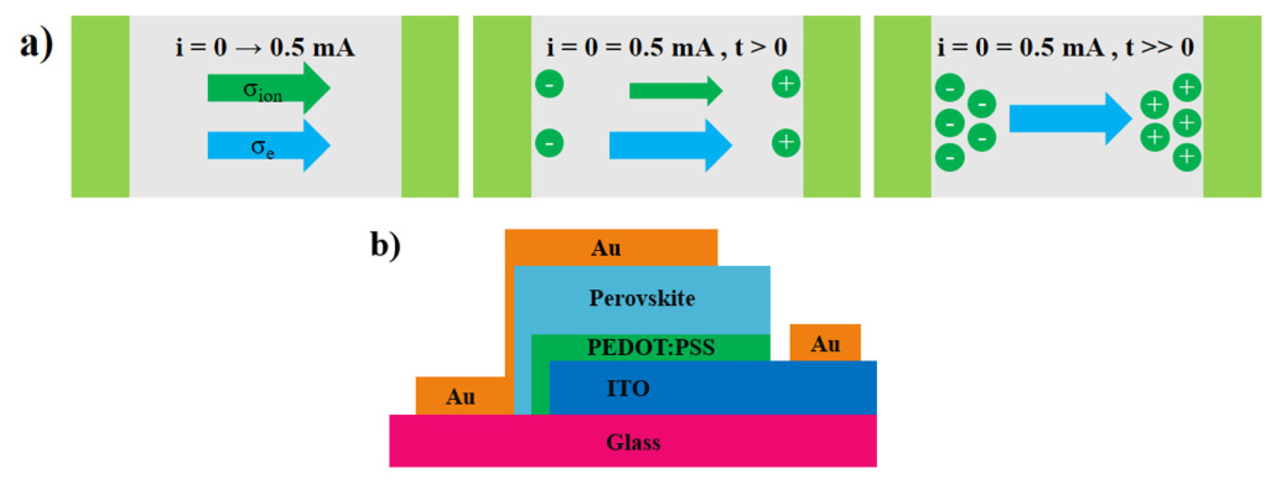
Several experimental techniques have been used to discover evidence of ion migration, such as photo thermal-induced resonance microscopy (PTIR) [12], Tubandt method [13], impedance spectroscopy [14], time of flight secondary ion mass spectrometry (TOF-SIMS) [15], electrochemical, and selective blocking [16,17]. Selective blocking measurement is easily accomplished and can be conducted at low temperatures. This method allows the separation of ion conduction from total conductivity [16]. A constant current is applied to measure the steady-state of voltage as a function of time; thus, electron and ion conductivity can be extracted [17]. Initially, both ions and electrons pass through the perovskite film. Then, the number of passing ions is reduced until only electrons directly pass through the perovskite film (Fig. 1a) [16].
In this study, ionic activation energies of the perovskite films MAPbI3, FAPbI3, CsPbI3, and MAPb-Br3, were measured using the selective blocking method. Ionic activation energy is influenced by crystal structure, radius of ion, and charge of ion [4]. For MAPbI3, the migrating ions might be I−, Pb2+, MA+, or H+ [4,18]. If cation MA+ is substituted into FA+ and Cs+, these ions may also migrate in the perovskite film. The ion migration in FAPbI3 can be suppressed by FA+, which has a larger diameter than MA+ [15]. Substitution of MA+ with monovalent cation Cs+ can eliminate the effects of ion migration enhancement due to light intensity in MAPbI3 [17]. Anion substitution of I− into Br− may provide another insight because Br− is also predicted to play a role in ion migration. Understanding ion migration makes it possible to design a new strategy to improve the stability of perovskites film.
2. Experimental
2.1 Fabrication of vertical devices
The structure of a vertical device is illustrated in Fig. 1b. This sandwich-like structure consisted of indium tin oxide (ITO), poly-(3,4-ethylene dioxythiophene): poly(styrene sulfonic acid) (PEDOT: PSS), a perovskite film, and gold. ITO glass was cut into 1×1 inch. A distance of 7 mm from one of the edges was etched using Zn powder and HCl solution to remove the ITO layer. ITO glass was cleaned by sonication in acetone, isopropyl alcohol, and deionized water for 10 min each. The cleaning process was continued by oxygen plasma for 20 min to improve the adhesion between the substrate and thin film.
PEDOT: PSS was filtered using 0.45 μm syringe filter then spin-coated onto clean ITO at 4000 rpm for 15 s and ramp 5.0. PEDOT: PSS layer was dried on the hot plate for 15 min at 125°C. The deposition process was performed in ambient air. On the top of PEDOT: PSS layer, perovskite solution (MAPbI3, MAPbBr3, FAPbI3, or CsPbI3) was spin-coated at 1000 rpm for 40 s, ramp 5.0, and 5000 rpm for 20 s. During spin-coating of MAPbI3, FAPbI3, CsPbI3, at t = 64 s, 800 μL of toluene was dropped on the top of perovskite film. For MAPbBr3, the toluene was dropped at t = 57 s. Toluene acted as an antisolvent for precursor; therefore, toluene drip facilitated fast crystallization of perovskite film. The perovskite film was dried on the hot plate for 10 min at 100°C for MAPbI3, 170°C for FAPbI3, 350°C for CsPbI3, and 75°C for MAPbBr3. The deposition process was conducted under N2 gas inside a glove box. Finally, an 80 nm Au layer was deposited on the top of the perovskite layer using a thermal evaporator at a rate of 1 Å/s.
2.2 Sample characterization
X-ray diffraction measurements (XRD) were carried out using Rigaku X-MAX from 10°–40° to examine the structure of each perovskite material. The vertical structure of each sample was confirmed by cross-section observation using Field Emission Scanning Electron Microscope (FE-SEM) MAIA III TES-CAN and JEOL JSM-6701F.
2.3 Selective blocking measurement
Selective blocking measurements were performed by a four-point probe system with a Faraday cage and a black shield. The black shield provided a dark condition for the measurement because, in this condition, ions migrate faster than electrons. The four-point probes were connected to the AutoLab controller with the PGSTAT302N module. NOVA Metrohm Autolab B.V version 1.10.1.9 was used as software. During measurement, two probes were connected to the cell. Hot chuck MH4R and controller MST 1000 H were used to control the temperature of the sample. Chronopotentiometry (Δt >1 ms) was used to characterize the sample in a 100 nA current flow for 20 s. The voltage-time (V-t) curve from that measurement was then used to calculate total resistance and electronic resistance. Finally, the resistivity and conductivity of both electrons and ions can be obtained.
3. Results and Discussions
3.1 Characterization of materials and devices
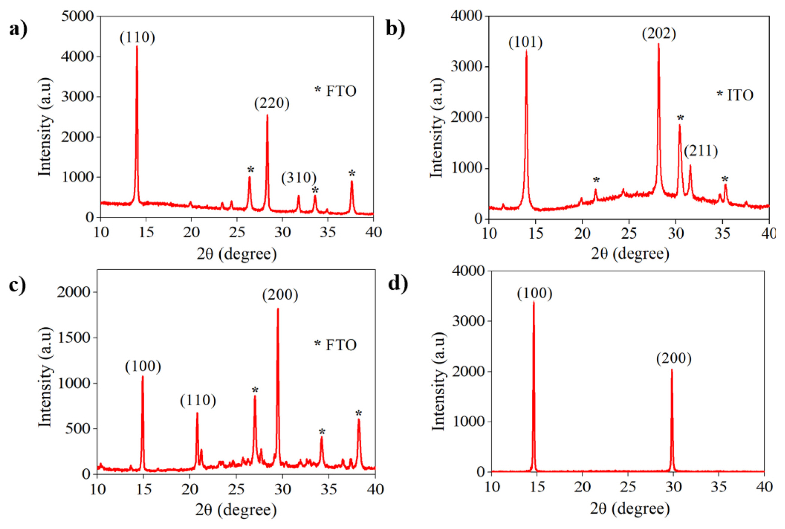
X-ray diffraction measurements were conducted to examine the perovskite structure. Each perovskite solution was deposited onto ITO or FTO glass without Au and PEDOT: PSS layer. The structure of each perovskite is presented in Fig. 2a–d. Fig. 2a shows (110), (220), and (310) peaks corresponding to the formation of orthorhombic MAPbI3 [19,20]. Fig. 2b confirms the formation of FAPbI3, showing (101), (202), and (211) peaks, which are assigned to trigonal α-FAPbI3 or black phase FAPbI3 [21,22]. Fig. 2c shows maximum intensity for (100) and (200), indicating the cubic black phase of CsPbI3, and the lower peak (110) indicates strain in the crystal structure [23,24]. In Fig. 2d, peaks of (100) and (200) correspond to MAPbBr3 with cubic formation [25].
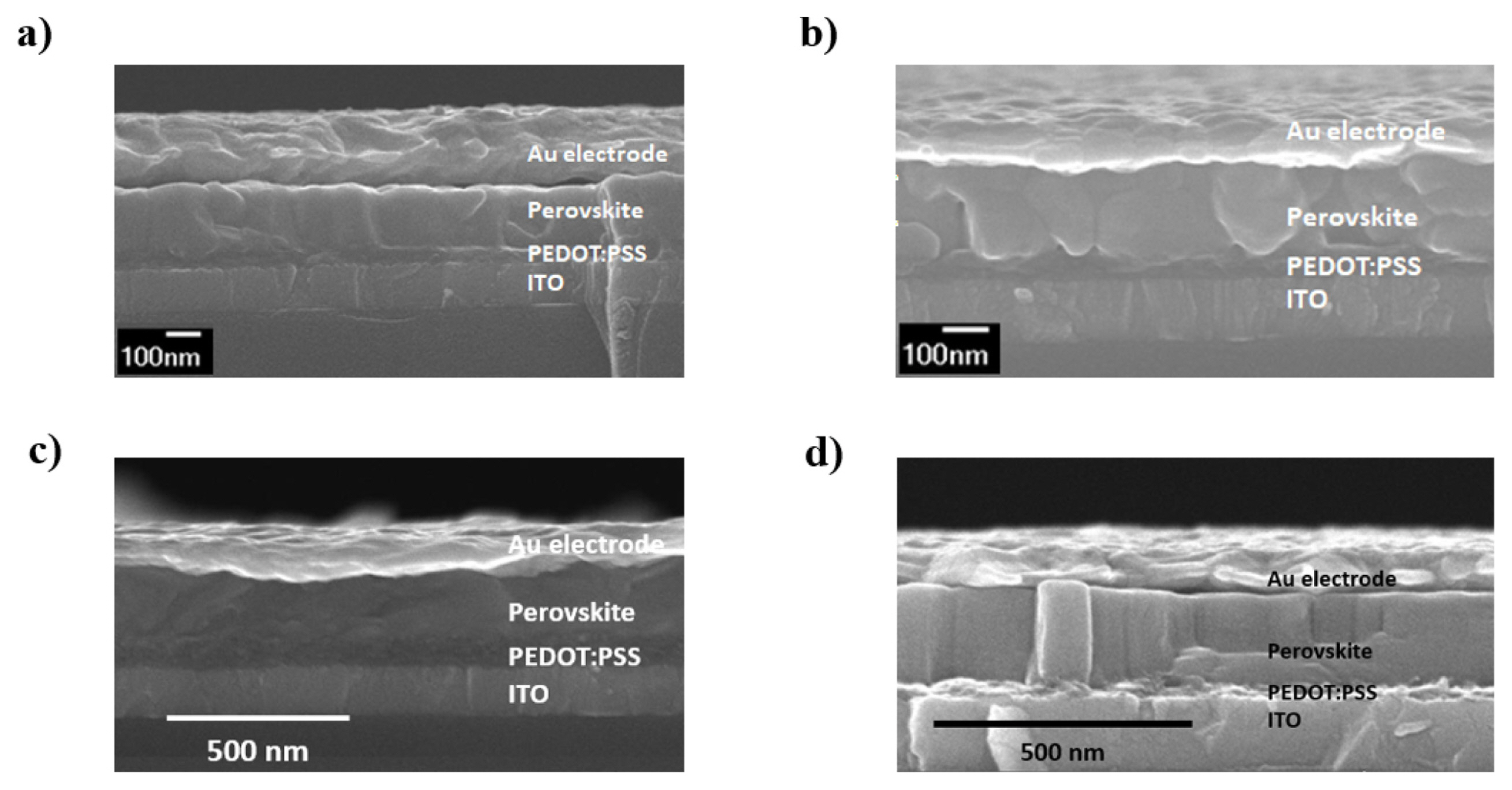
FE-SEM confirmed the vertical structure of the device. The devices were constructed like a sandwich (ITO/PEDOT: PSS/perovskite/Au) with perovskite as an active layer. FE-SEM images are presented in Fig. 3a–d.
Cross-section images show that all layers are presented and vertically stacked. The perovskite thickness was approximately 200 nm. Using the Scherrer equation, average grain size can be calculated from XRD peaks. The average grain size for MAPbI3 is 43 ± 3 nm. CsPbI3 has a larger grain size of 51 ± 4 nm. MAPbBr3 has the largest average grain size (55 ± 4 nm), whereas FAPbI3 has the smallest average grain size (29 ± 7 nm). These average grain sizes are much lower than other groups whose minimum grain sizes are approximately 300 nm [26,27].
3.2 Selective blocking
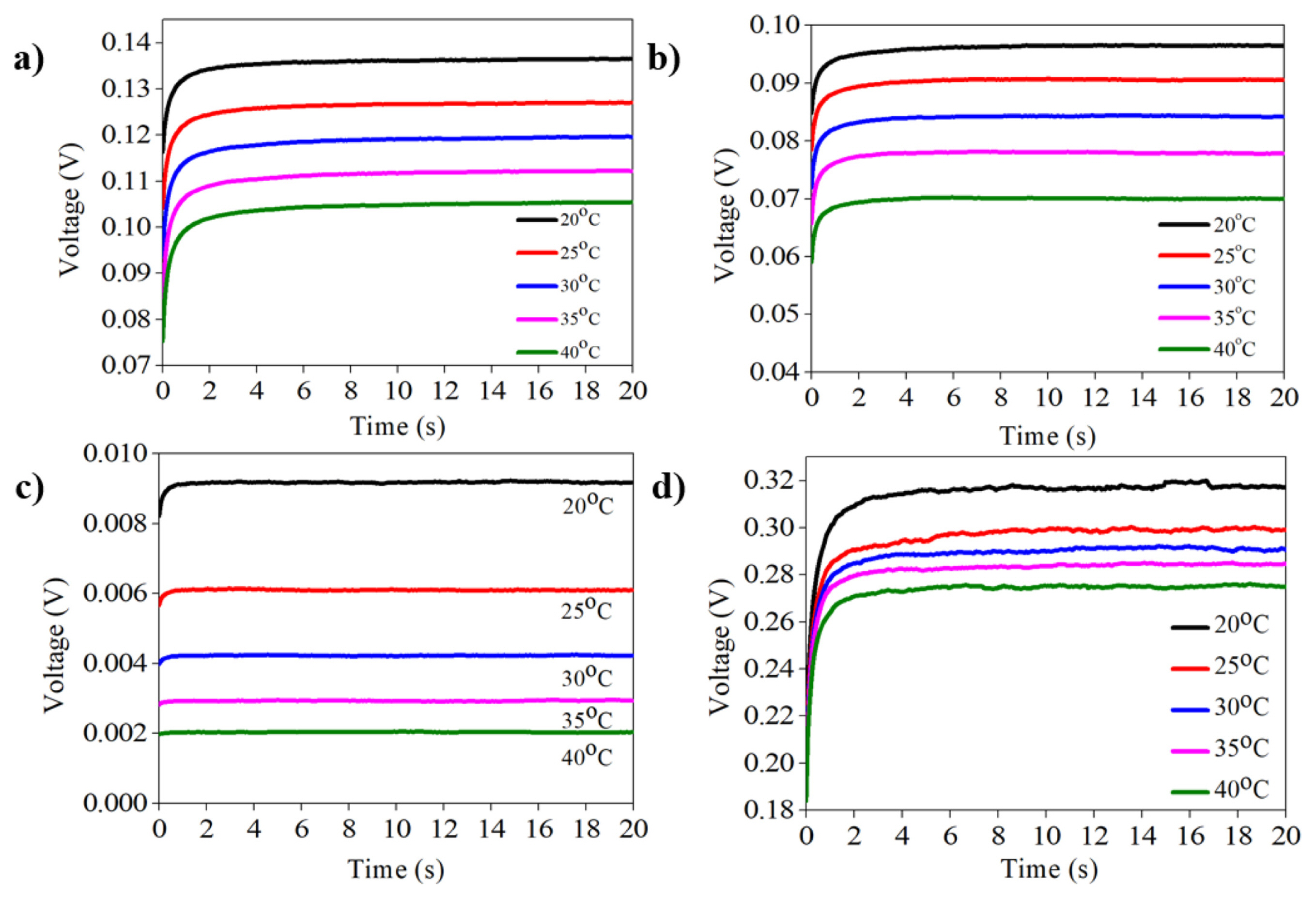
Selective blocking measurements were performed in the dark, and ionic conductivities were measured. When a constant current was applied to the vertical device, the potential difference between two terminals was measured as a function of time. The potential difference was affected by electronic resistance (Re) and ionic resistance (Rion), which can be written as Eqn. (1) [13]:
As ions keep migrating in one direction, the ions were depleted at one end and accumulated at another end. In this stage, only electrons migrated, which correspond to i = ie and iion = 0 [13]. Thus, the voltage can be written as Eqn. (2) :
By measuring the initial and final voltages, and combining Eqn. (1) and (2), Re and Rion can be determined. Furthermore, the ionic (σion) and electronic conductivities (σe) can be calculated from Rion and Re. In this study, each sample was measured at room temperature (20–40°C), which perovskite devices operate typically.
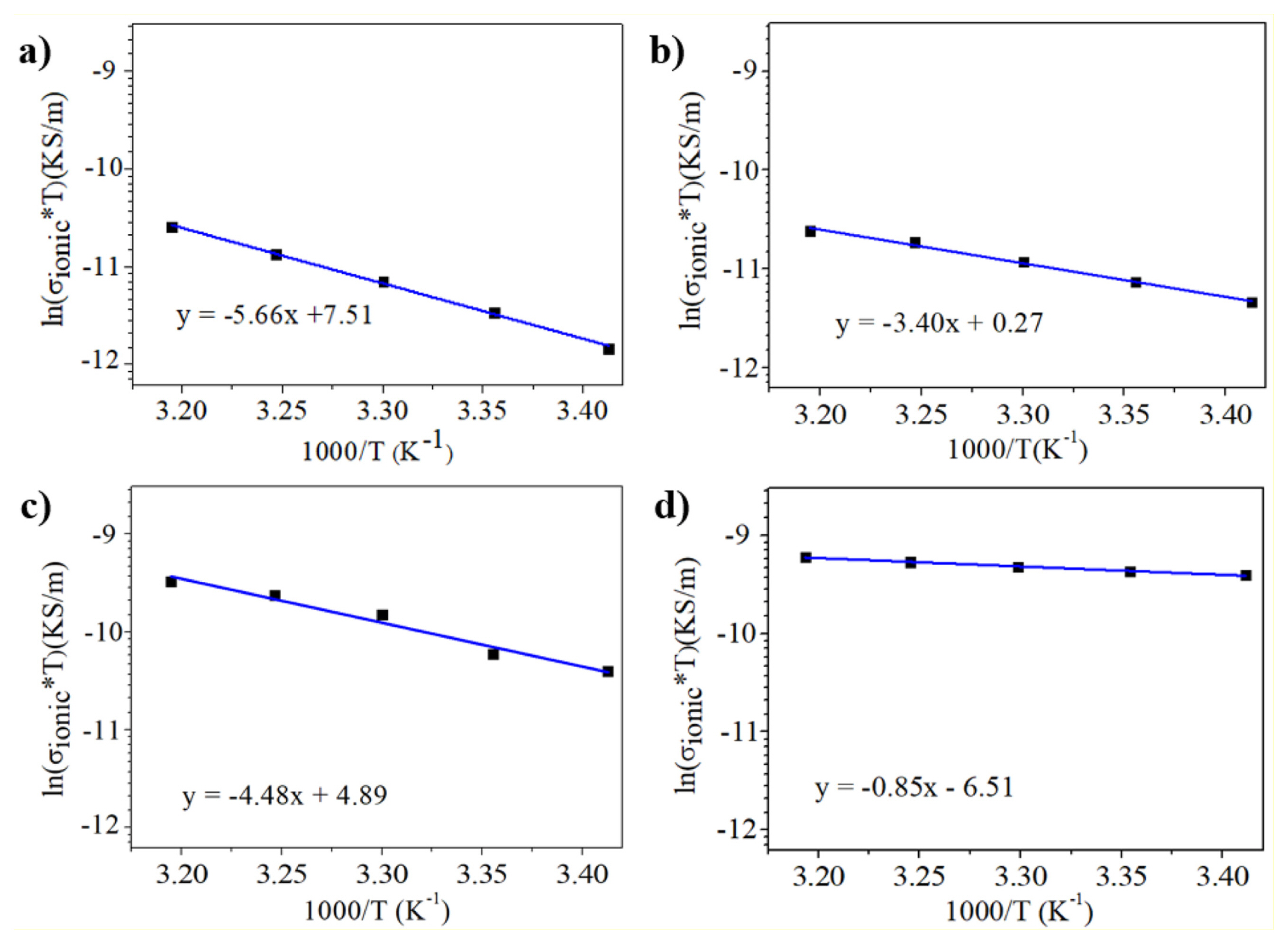
Fig. 4a–d show the voltage-time (V-t) graphs from selective blocking measurements for various perovskite materials, which show typical behavior of mixed conduction of electrons and ions. At the current onset, perovskite film exhibits a lower resistance because both ionic and electronic conduction occurs. However, as the ionic conduction is blocked at the interface between the perovskite and metal electrode, the resistance is gradually increased and reaches a steady-state level, where ionic conduction is completely blocked, and only electrons can flow. On the other hand, when the temperature is increased, the resistance of the perovskite is decreased because charge carriers (electrons and ions) are thermally activated. Using the Arrhenius relation between the conductivity and temperature, the activation energy (Ea) for conduction can be obtained as shown in Fig. 5a–d.
3.3 Ionic activation energy
Activation energy (Ea) is the minimum energy that must be overcome by an ion to jump from its initial position to nearby vacancy sites [26]. After calculating ionic conductivities at each temperature, these values can be further processed to extract the Ea value for each perovskite materials. Following Arrhenius dependence, ionic activation energy can be calculated using Eqn. (3) [17]:
where σi is conductivity, σ0 is the pre-exponential factor, Ea is the activation energy, kb is Boltzmann constant, and T is temperature. That equation can be rearranged into Eqn. (4):
In Fig. 5 ln(σiT) versus 1/T is plotted, and a linear fit is applied. The slope corresponds to
- E a k b
The measured Ea value for MAPbI3 (0.48 eV) is close to those from previous literature, which is 0.43 eV [13] and 0.45 eV [28]. According to a study using density functional theory (DFT) calculation, the activation energy of I− is 0.58 eV [29]. It is assumed that I− has the shortest pathway to I− vacancies through the edge of PbI6 octahedron. In contrast, Pb2+ has the longest pathway because it needs to pass along the diagonal direction <110>. Meanwhile, MA+ migrates to the nearest V’MA cage of the unit cell face composed of four I ions. Both Pb2+ and MA+ have longer paths than I−; thus Pb+ (2.31 eV) and MA+ (0.84 eV) have higher activation energies than I− (0.58 eV) [29].
The Ea value for MAPbBr3 (0.073 eV) in Table 1 has important implications in identifying the migrating species in the perovskite materials. With the substitution of I− with Br−, MAPbBr3 has a much lower Ea value than MAPbI3 (0.48 eV). The lowered Ea for the anion –substituted perovskite indicates that the migrating species might be the anion. As the ionic radius of Br− (0.196 nm) is smaller than I− (0.220 nm), Br− will more easily migrate in the perovskite crystal despite the lattice size of the Br− substituted perovskite in smaller than generic material. In contrast, other groups suggested that according to computational study, Br− has comparable energy activation to I− [30,31].
In this study, we also investigated cation substitution by substituting MA+ with FA+ and Cs+. The experimental result showed that FAPbI3 (0.29 eV) has lower ionic activation energy than MAPbI3 (0.48 eV). Noting that FA+ (0.253 nm) is larger than MA+ (0.216 nm), the observed reduction of Ea value for FAPbI3 can be explained by the fact that FAPbI3 has a larger lattice constant, leading to a lower barrier for I migration. For CsPbI3, even though the ionic radius of Cs+ is smaller than MA+ and the smaller crystal might increase the barrier for I− migration, the measured Ea value is smaller than that for MAPbI3. This result is not clearly understood yet. We expect that other factors than crystal lattice size might come into play, such as simultaneous cation (Cs+) migration or ion migration along the grain boundary.
In this experiment, a perovskite film was fabricated by a solution process followed by annealing, which allowed evaporation of solvent after spin coating. Consequently, grain boundaries were generated on the surface, which might have facilitated ion migration. If the ion migrates in the grain boundaries, the ionic activation energy is only half of the ionic activation energy from ion migration in bulk [4]. Therefore, the low ionic activation energy of metal halide perovskite in this experiment compared to others might have been caused by the abundance of grain boundaries.
4. Conclusions
Ion migration in metal halide perovskite was investigated by measuring ionic activation energy. The ionic activation energies from the vertical structure devices of MAPbI3, MAPbBr3, FAPbI3, and CsPbI3 were examined using selective blocking. The ionic conductivity was extracted from mixed conductivity at 20°C to 40°C. The calculated ionic activation energy from MAPbI3, FAPbI3, CsPbI3, and MAPb-Br3, are 0.49 eV, 0.29 eV, 0.39 eV, and 0.07 eV, respectively. These values were compared with other results in the literature. Variations in ionic activation energy are understandable because every research group has different experimental techniques, fabrication processes, and measurement conditions. This study found that I− is a possible ion that migrates in MAPbI3, FAPbI3, and CsPbI3, whereas Br− is the most mobile ion in MAPbBr3.