


1. Introduction
The discovery of graphene has led to significant developments in the field of supercapacitors [1]. In particular, the 2D structure of graphene is highly advantageous in ultra-small energy storage devices that store a large amount of charge over an infinitesimal volume [2-7]. In our previous report, we introduced graphene-based electrodes with an in-plane structure, in which electrolyte ions interact with the graphene layers in the electrode, thereby maximizing the utilization of the electrochemical surface area [7]. Following this report, the effectiveness of in-plane-structured graphene as a supercapacitor electrode material has been acknowledged in the literature. Further, a number of studies have reported the successful use of this structure in improving ion transport in ultra-small supercapacitors, which leads to improved power and capacitance [2-7]. However, the difference between the volumetric capacitances of multilayer graphene electrodes with in-plane and out-of-plane (conventionally stacked) structures has not yet been definitively evaluated. This information could reveal both the potential of the in-plane structure as well as limitations of the out-of-plane structure and would thus be helpful in the design of efficient electrodes for the fabrication of high-performance supercapacitors.
In the present study, we employ reduced multilayer graphene oxide (RMGO) films as the supercapacitor electrode material and compare the volumetric capacitances of planar supercapacitors with the in-plane structure (hereafter referred to as in-plane-structured devices) and conventionally stacked supercapacitors with the out-of-plane-structure (referred to as out-of-plane-structured devices hereafter). The aim of this study is to confirm the potential of in-plane-structured graphene as an electrode material for ultrasmall energy storage devices with high volumetric capacitances.
2. Experimental
The RMGO films and the in-plane- and out-of-plane-structured devices were prepared as described in our previous report [7]. The RMGO films were prepared on quartz slides (TED PELLA, INC., USA) via a layer-by-layer (LBL) self-assembly method as follows. First, the graphene oxide (GO) film was prepared by a LBL assembly of GO and poly (ethyleneimine) (PEI). PEI, a cationic polymer, was purchased from Sigma-Aldrich (branched PEI: Mw 25,000). GO was synthesized from graphite powder (SP-1, Bay Carbon, MI) using the modified Hummers method. The aqueous solutions had concentrations of 1 wt% for PEI and 0.02 wt% for GO. Subsequently, the self-assembled GO film was heat-treated at 350┬░C for 1 h to remove the cationic polymers and chemically reduced with a 0.1 wt% aqueous solution of hydrazine hydrate (64%, Acros) at 50┬░C for 30 min to form the desired RMGO films. These films were then employed in both kinds of devices [7].
3. Results and Discussion
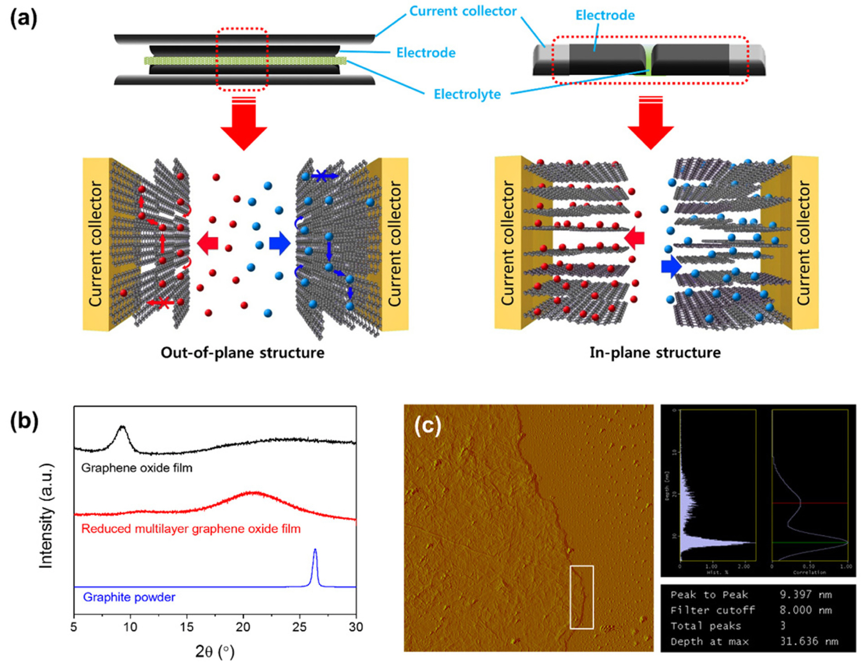
Figure 1a presents a schematic representation of both the in-plane- and out-of-plane-structured supercapacitors, where the out-of-plane-structured device is a conventionally stacked supercapacitor with the basal planes of graphene facing one another. In this case, the RMGO films on the two different quartz slides are stacked with the polymer-gel electrolyte sandwiched between them. In contrast, the in-plane-structured device is a planar-type supercapacitor with the edge planes of graphene facing one another. This device also employs RMGO films and a polymerŌĆōgel electrolyte. The in-plane-structured devices consist of two planar RMGO electrodes (2 ├Ś (1 mm ├Ś 20 mm)) whose edge planes face one another and are separated by a small gap of approximately 60 ╬╝m. In addition, gold was sputtered on both edges of the RMGO film to act as the current collector, and the polymerŌĆōgel electrolyte, composed of a 5:4 mixture (by weight) of poly(vinyl alcohol)/phosphoric acid (H3PO4), was applied on the active area of the electrodes. In contrast, during preparation of the out-of-plane devices, the RMGO films were prepared on two separate quartz slides. Following application of the polymer-gel electrolytes onto the electrodes and subsequent drying, the two electrodes were stacked and gently pressed together. The thickness of the polymer-gel electrolyte was adjusted to approximately 60 mm. Then, cyclic voltammetry (CV) was conducted to evaluate the electrochemical performances of the devices using a VSP potentiostat (Bio-Logic Science Instruments) with a two-electrode system. Finally, atomic force microscopy (AFM, Nanoscope IIIa AFM, Digital Instrument-Vecco) and X-ray diffraction (XRD, D/MAX RC, Rigaku) were conducted to determine the thicknesses and structures of the RMGO films, respectively.
As shown in the XRD profile in Figure 1b, the (002) plane of the as-prepared GO film exhibited a strong, sharp peak at 2╬Ė = 9.3┬░, which shifted to 21.1┬░ (d = 4.2 ├ģ) on chemical reduction of the GO film. This peak shift indicated that the GO film was successfully reduced by chemical reduction. In particular, the presence of the peak corresponding to the graphite (002) plane at a higher 2╬Ė value of 26.5┬░ (d = 3.4 ├ģ) supported the conclusion that the interlayer distance in the RMGO film was higher than that in graphite. This difference might be attributed to the outgassing of PEI, water molecules, and other functional groups during heat treatment [7]. As shown in Figure 1c, AFM surface measurements confirmed that the RMGO film was approximately 10 nm thick (10.4 ┬▒ 0.89 nm) and that the surface exhibited a smooth morphology with some small blemishes.
Fig.┬Ā1.
Device geometry and material characteristics. (a) Schematic depiction of the conventionally stacked device with an out-of-plane structure and the planar type device with an in-plane structure. The red and blue spheres indicate cations and anions, respectively. (b) X-ray diffraction profiles for the graphene oxide (GO) films (top, prepared using the layer-by-layer method), reduced multilayer graphene oxide (RMGO) films (middle, prepared by subsequent heat treatment and chemical reduction of the GO films), and commercial graphite powder (bottom). (c) Representative atomic force microscopy image and depth profiles of the RMGO film on a mica substrate. Several regions of the RMGO films were subjected to depth profile and line scan analyses. An approximate thickness of 10 nm (10.4 ┬▒ 0.89 nm) was revealed.
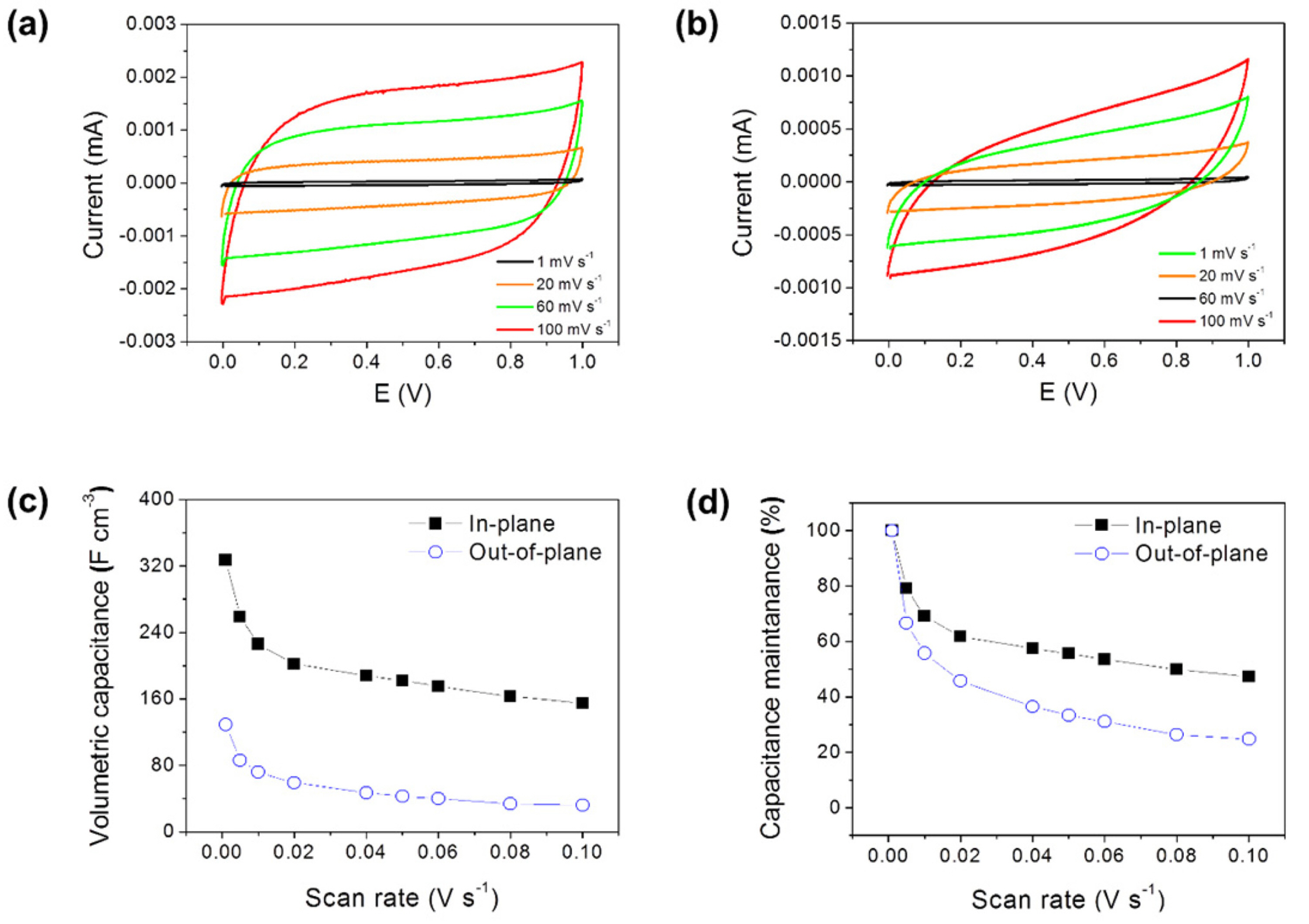
The electrochemical capacitance characteristics of the two types of devices were evaluated, and the results are shown in Fig. 2. CV curves of the in-plane- and out-of-plane-structured devices were measured at various scan rates in the range of 1-100 mV sŌłÆ1. As shown in Fig. 2a, the CV curves of the in-plane-structured devices were nearly rectangular, even at very high scan rates, indicating that the electric double layer (EDL) was efficiently established in both electrodes. However, in the case of the out-of-plane-structured device, the CV curves deviated significantly from the rectangular shape, indicating that the EDL was not established efficiently (Fig. 2b). The capacitance values were then calculated by integrating the discharge area under the CV curves. All formulae employed for these calculations are presented in the Supplementary Material. Assuming symmetry for the RMGO electrode in the in-plane-structured device, the volumetric capacitance of one electrode, Cvol, was calculated from the device capacitance to be 327 F cmŌłÆ3 (Figure 2b, Table 1). In contrast, the volumetric capacitance of the RMGO electrode in the out-of-plane-structured device was calculated to be 129 F cmŌłÆ3 (Figure 2c, Table 1). These results indicate that the capacitance of the in-plane-structured RMGO film was 2.5 times larger than that of the out-of-plane-structured RMGO film. Indeed, the volumetric capacitance for the in-plane-structured device reported herein is the highest among the values reported for any graphene-based ultra-small supercapacitor. Although our device is too thin to be applied for practical use, it is noteworthy that we have demonstrated the potential of in-plane-structured graphene as a supercapacitor electrode material. Additionally, the variation in the capacitance maintenance with the scan rate (shown in Figure 2d) clearly demonstrates more efficient electrolyte ion transport in the in-plane configuration than in the out-of-plane configuration.
Table┬Ā1.
Physical dimensions and electrochemical performance evaluation of the in-plane- and out-of-plane-structured reduced multilayer graphene oxide supercapacitors.
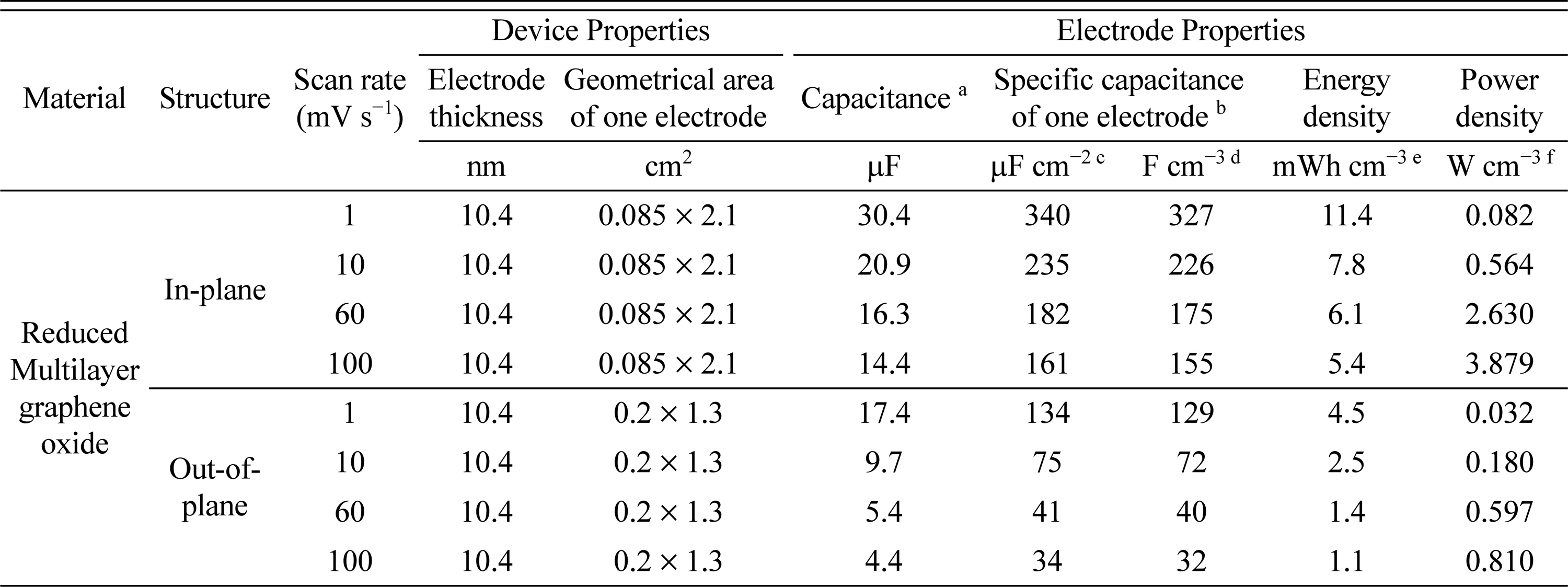
a The capacitance values correspond to the best performance obtained using the discharged area of the cyclic voltammetry curves.
b Specific capacitance of one electrode calculated from the device capacitance, assuming a symmetrical capacitor.
c Normalized by the geometrical area of one electrode.
d Normalized by the volume of one electrode (electrode thickness ├Ś geometrical area of one electrode).
e Normalized by the volume of both electrodes.
f Normalized by the volume of both electrodes.
Fig.┬Ā2.
Electrochemical performances of the reduced multilayer graphene oxide electrodes. (a) Cyclic voltammetry (CV) curves obtained at different scan rates for the planar-type supercapacitor with an in-plane structure. (b) CV curves obtained at different scan rates for the stacked supercapacitor with an out-of-plane structure. (c) Comparison of the volumetric capacitances of the in-plane- and out-of-plane-structured devices with increasing scan rates. (d) Comparison of the rates of capacitance maintenance of the in-plane- and out-of-plane-structured devices with increasing scan rates.
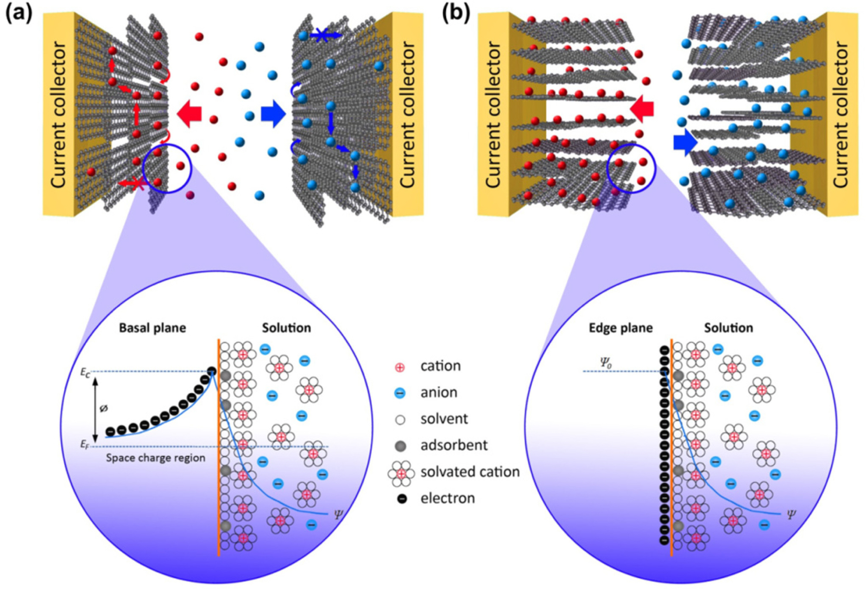
As shown in Fig. 3a, the graphene layers were stacked parallel to the current collector in the out-of-plane geometry. Consequently, the electrochemical surface area was incompletely utilized because some of the regions were inaccessible to the electrolyte ions and because ionic transport was limited within the graphene layers. This led to a lower volumetric capacitance in the stacked device and, as such, this geometry was unfavorable for maximizing the device performance. In addition, owing to the limited ion transport and incompletely utilized electrochemical surface area, the CV curve deviated significantly from a rectangular shape. Furthermore, the capacitance value was low and could not be maintained at high scan rates. In contrast, in the planar-type device with the in-plane structure, the transport of electrolyte ions in the graphene layers was enhanced, allowing the EDL to be efficiently established, thus leading to improved utilization of the electrochemical surface area. In this case, the CV pattern was rectangular and the capacitance was 2.5 times larger than that of the stacked device with the out-of-plane structure. In this case, the capacitance value could be maintained, even at a high scan rate. Additionally, the low capacitance of the stacked device with the out-of-plane structure could also be attributed to the semiconducting properties of the RMGO layers along the direction of the basal orientation. Indeed, many studies have shown that the double-layer capacitance at the edges is higher than that on the basal layer of graphite [8-13]. This low capacitance on the basal plane can be accounted for by the semiconductive characteristics along the direction perpendicular to the basal plane. More specifically, low-density electronic states near the Fermi level cause a smaller capacitance in the space charge region compared to the EDL capacitance, which is related to the electrolyte. However, graphite behaves like a metal along the edge because the charge carrier density of graphite is similar to that of a metal [8-10,13,14]. Thus, the capacitance is larger along the edges than the basal plane. Based on the above explanation, the potential profiles at the basal plane and edge plane/electrolyte interface under a negative bias potential are shown in Figures 3a and 3b, respectively. The in-plane design tends to allow the electrolyte ions to be efficiently transported and, as such, permits their interaction with all RMGO layers. This therefore allows the high surface area offered by the graphene layers to be fully utilized. Furthermore, the in-plane structure allows the unique electrochemical properties at the edges of the graphene layers to be effectively exploited.
Fig.┬Ā3.
(a) Schematic depiction of the stacked device with an out-of-plane structure and the potential profile at the basal plane/electrolyte interface under a negative bias potential. Ec and EF are the potentials of the conduction band and Fermi level, respectively. (b) Schematic depiction of the planar device with an in-plane structure and the potential profile at the edge plane/electrolyte interface under a negative bias potential.
The overall performances of the in-plane- and out-of-plane-structured devices are summarized in the form of a Ragone plot, as shown in Fig. 4. The energy and power densities of the devices are compared with those of a thin-film Li battery, a commercial supercapacitor, and an electrolytic capacitor.[3] The in-plane-structured device exhibited an energy density of up to 11.4 mWh cmŌłÆ3, which exceeded that of the thin-film Li battery (approximately 8 mWh cmŌłÆ3) and is approximately 16-times higher than that of a commercial supercapacitor. In addition, the in-plane-structured device yields a power density of up to 3.9 W cmŌłÆ3, which is significantly higher than that of the thin-film Li battery and the commercial supercapacitor. This value is also comparable to the power density of Al electrolyte capacitors. Although the performance of the out-of-plane-structured device is significantly improved compared to that of the commercial supercapacitor, the energy and power densities of the out-of-plane-structured device are lower than those of the in-plane structured device. Overall, these results indicate that in-plane-structured graphene has enormous potential as a supercapacitor electrode material. The results of this study therefore pave the way to designing practical supercapacitors exhibiting high performances, in addition to energy densities close to that of Li thin-film batteries and power densities close to that of Al electrolytic capacitors.
Fig.┬Ā4.
Comparison of the energy (Wh cmŌłÆ3) and power (W cmŌłÆ3) densities of the in-plane- and out-of-plane-structured devices. The energy and power densities of alternative energy storage devices reported in the literature are also shown (e.g., a thin-film Li battery, a commercial supercapacitor, and an electrolytic capacitor [3]).

4. Conclusions
We studied the volumetric performance of reduced multilayer graphene oxide electrodes with in-plane and out-of-plane structures. The in-plane-structured device exhibited a volumetric capacitance of 327 F cmŌłÆ3, which is 2.5 times larger than that of the out-of-plane-structured device. Furthermore, the in-plane device exhibited an energy density of 11.4 mWh cmŌłÆ3, which is higher than that of lithium-ion thin film batteries. Thus, it is reasonable to conclude that the in-plane-structured graphene-based electrodes displayed sufficient potential for use as electrodes with high volumetric performances for ultra-small energy storage device applications. In the future, we intend to adopt the in-plane-structured electrode for use in thin-film-based supercapacitors because we expect that it will provide the volumetric energy density required for such applications.


