SnO2-Coated 3D Etched Cu Foam for Lithium-ion Battery Anode
Article information
Abstract
SnO2-based high-capacity anode materials are attractive candidate for the next-generation high-performance lithium-ion batteries since the theoretical capacity of SnO2 can be ideally extended from 781 to 1494 mAh g−1. Here 3D etched Cu foam is applied as a current collector for electron path and simultaneously a substrate for the SnO2 coating, for developing an integrated electrode structure. We fabricate the 3D etched Cu foam through an auto-catalytic electroless plating method, and then coat the SnO2 onto the self-supporting substrate through a simple sol-gel method. The catalytic dissolution of Cu metal makes secondary pores of both several micrometers and several tens of micrometers at the surface of Cu foam strut, besides main channel-like interconnected pores. Especially, the additional surface pores on etched Cu foam are intended for penetrating the individual strut of Cu foam, and thereby increasing the surface area for SnO2 coating by using even the internal of Cu foam. The increased areal capacity with high structural integrity upon cycling is demonstrated in the SnO2-coated 3D etched Cu foam. This study not only prepares the etched Cu foam using the spontaneous chemical reactions but also demonstrates the potential for electroless plating method about surface modification on various metal substrates.
1. Introduction
To meet the growing needs for various applications of energy storage, the development of high-performance electrode materials with higher energy density and better cycle life has been stimulated, which enables the SnO2-based high-capacity anode materials to become a promising candidate for the high-performance lithium-ion batteries (LIBs) [1–3]. Compared to the graphitic carbon in most commercial LIBs with the limited theoretical capacity of 372 mAh g−1 in forming the LiC6, the SnO2 has attracted attention due to the high theoretical capacity of 781 mAh g−1 in forming the Li4.4Sn [4–6]. In particular, the theoretical capacity of SnO2 can be extended ideally to 1494 mAh g−1 by achieving the complete conversion reaction for forming the re-formed SnO2 upon charge process [5,6]. However, the large amounts of lithium stored during discharge and charge processes inherently induce large volume expansion and contraction of ~ 300%, causing a pulverization of electrode materials and a loss of electrical contact, and eventually resulting in poor battery performance [5,6].
Substantial efforts have been dedicated for addressing the issue of large volume changes in SnO2 anode material, especially through the unique nano-structuring of high-capacity material combined with the integrated electrode design wherein both the void space for alleviating the volume changes and the current collector integrated, and binder- and carbon-agent free electrode for having the structural integrity can be achieved [7–14]. Among the various morphology controls of high-capacity materials from zero-dimensional (0D) to three-dimensional (3D), the 3D architectures such as inverse opal scaffold [7,8], nanofoam [9–12], and long chains of particles [13,14] have attracted great attention as a smart electrode prototype. To obtain the stable and high energy density in the SnO2 electrode by using the 3D integrated electrode concept, in our previous reports we prepared the two types SnO2-coated Cu foams, using commercially available Cu foam and freeze-casting-derived Cu foam, through sol-gel coating method [10,11]. Compared to the conventional SnO2 nanoparticle electrode, the superiority of 3D inter-connected Cu scaffolds was demonstrated in the high lithium storage and also the rate capability, by preserving their original architecture upon cycling.
Herein, we prepared 3D etched Cu foam using an electroless plating method wherein spontaneous reactions in aqueous solution were applied to the non-galvanic electroless plating, known as the chemical and auto-catalytic plating method [15]. After that, the 3D etched Cu foam was applied as the current collector for electron path and also the substrate for SnO2 coating. In particular, the additional surface pores on etched Cu foam were intended for penetrating the individual strut of Cu foam, and thereby extending the surface area for SnO2 coating into the internal of Cu foam. By introducing the surface area-increased 3D Cu substrate in this study, the areal capacity was enhanced with high retention of structural integrity during cycling, which delivers the potential for electroless plating method about surface modification on various metal substrates.
2. Experimental
Commercially available Cu foam purchased from Korea Metalfoam company was punched 12 mm in diameter for fitting electrode size with 500 μm of thickness. For applying electroless plating, the punched Cu foam was immersed in 10 mL of 0.1 M AgNO3 acid solution under sonication during 1 min, and washed with deionized water (DI-H2O). The etched Cu foam was dried at 100 C in vacuum for 24 h, and a heat treatment was carried out at 500°C under H2 atmosphere during 5 h for a reduction of copper oxide to metallic copper in the etched Cu foam. After that, for a SnO2 coating process, the solgel method based on our reports for the fabrication of SnO2-coated Cu foam was applied also in this study [10,11]. The commercially available Cu foam, the Cu foam after etching by the electroless plating, the Cu foam after the H2 heat-treatment, and the Cu foam after the SnO2 coating were referred to as Pristine Cu foam, Etched Cu foam, Etched Cu foam after H2, and SnO2/Etched Cu foam, respectively. The SnO2/ Etched Cu foam was used as a working electrode without any binding and conductive materials.
X-ray diffraction (XRD) patterns were collected by Bruker D2 PHASER diffractometer with Cu Kα1 radiation (λ=1.54056 Å) in the range of 20–80°. The morphologies of electrode were characterized by using field-emission scanning electron microscopy (FE-SEM, JEOL JSM7000F). X-ray photoelectron spectrometer (XPS) measurement was conducted using VG microtech (ESCA, 2000) with a monochromatic Al Kα source, and the results were calibrated by referencing C 1s at 284.6 eV. Pore size distribution of the Cu foam was analyzed using mercury intrusion porosimetry (AutoPore IV 9510, Micromeritics), wherein the equipment specification for MIP test could reliably detect the pores from several μm to ~100 μm in diameter. A 2032 coin cell, consisting of the SnO2/Etched Cu foam as a working electrode, lithium metal as counter and reference electrodes, and polypropylene separator, was assembled in glove box under Ar atmosphere. Electrolyte in this study was 1.3 M LiPF6 dissolved in the mixture of diethyl carbonate (DEC) and ethylene carbonate (EC) with 1:1 (v/v). Galvanostatic evaluations (WBCS3000 cycler, WonA Tech, Korea) were conducted in voltage range of 0.01–3 V.
3. Results and Discussion
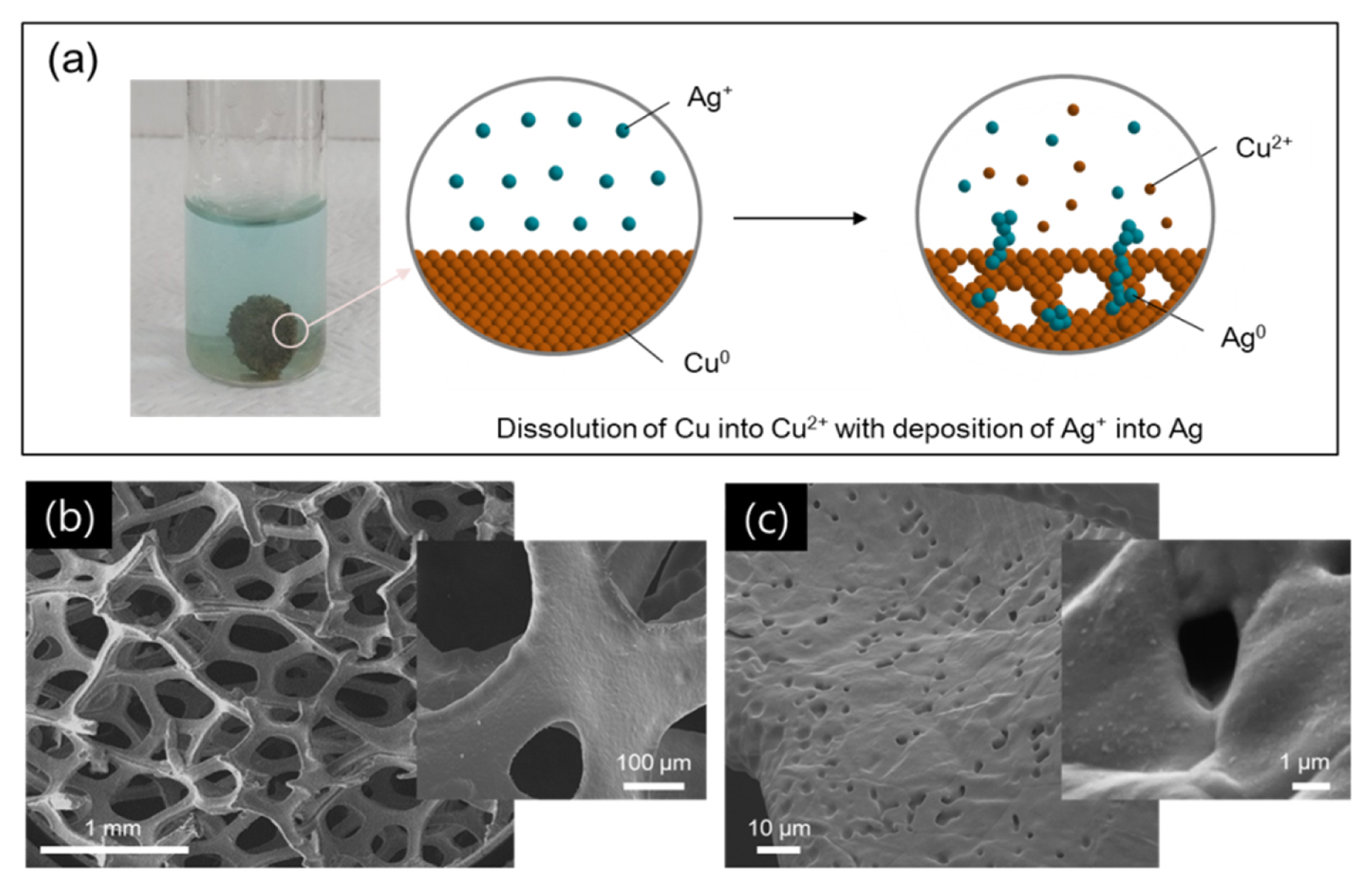
Fig. 1a depicts the fabrication of the etched Cu foam by using the electroless plating method. The commercially available Cu foam is immersed into the 0.1 M AgNO3 acid solution, and thereby spontaneous chemical reactions, dissolution of copper metal into Cu2+ and deposition of silver ion into Ag, occur in the aqueous solution without use of external electrical power [15]. Besides the inevitable Ag plating at the surface of Cu foam, the dissolution of Cu metal will make a formation of surface pore that penetrates the strut of Cu foam, and accordingly allow the use of internal surface of the Cu foam. Fig. 1b shows the morphology character of the commercially available Cu foam at the pristine state prior to the etching process. The Cu foam is a 3D scaffold composed of continuous struts of ~100 μm width and of interconnected pores of 100–500 μm diameter. The surface of the pristine strut is further examined at higher magnification as shown in the inset of Fig. 1b, and smooth surface condition is observed at the pristine state. However, after the etching process many small pores are developed at the surface of the Cu foam strut through the dissolution of Cu metal into Cu2+ as shown in Fig. 1c. It is confirmed that these pores with several micrometers in diameter penetrate the Cu foam strut as shown in the inset of Fig. 1c. Furthermore, the small and white dots on the surface of Cu foam can be indicative of the Ag deposition as illustrated in Fig. 1a.

(a) Schematic illustration for etching process at Cu foam surface, and SEM images of (b) pristine Cu foam and (c) etched Cu foam after etching process. Each inset shows the Cu surface at higher magnification.
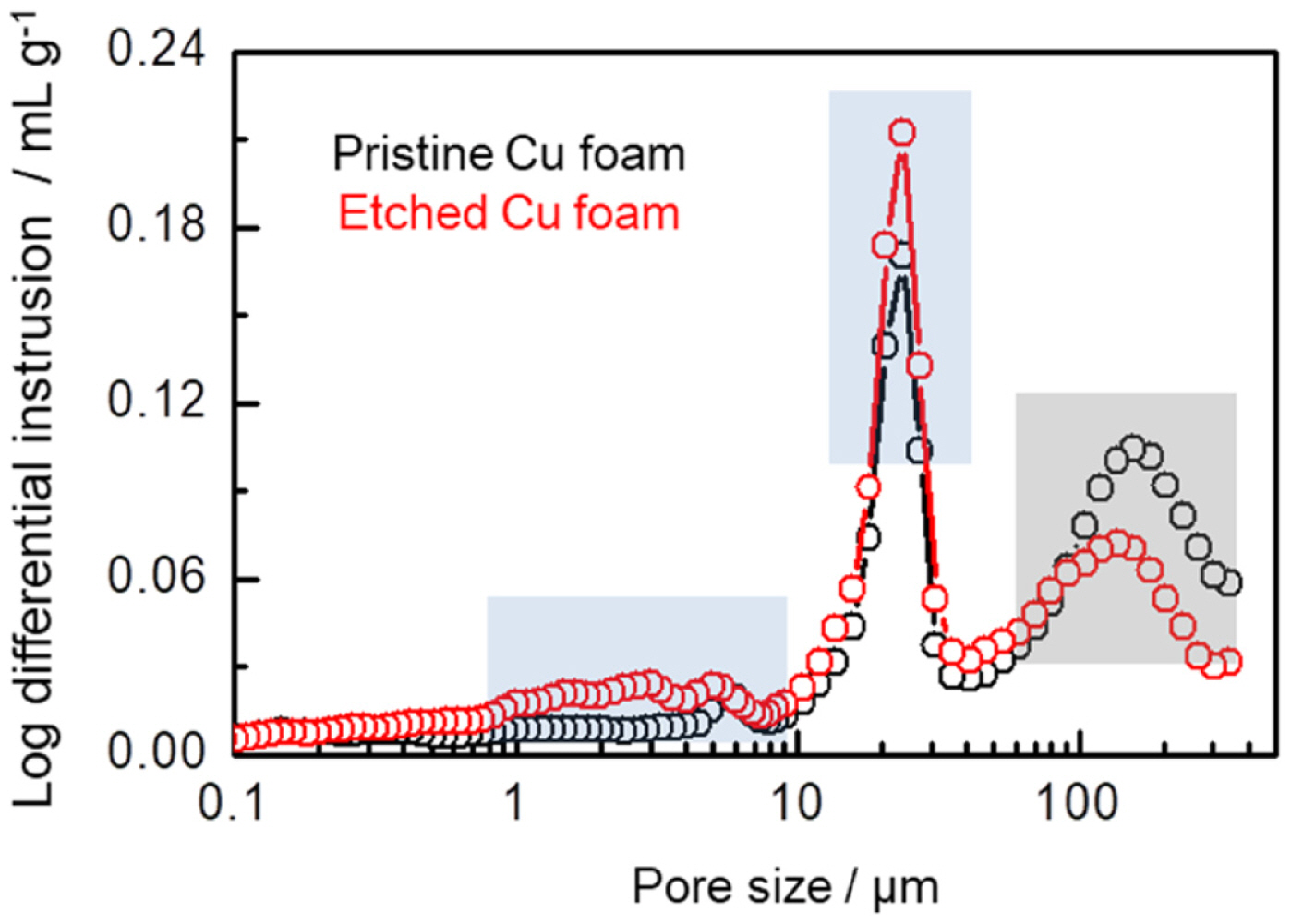
To evaluate the development of porosity for the Cu foam after the etching process, a mercury intrusion porosimetry (MIP) analysis was carried out in Fig. 2. Compared with the pristine Cu foam, the secondary pores of both several micrometers and several tens of micrometers develop at the surface of the strut after the etching process, in qualitative agreement with the SEM image in Fig. 1c. Because the MIP test could reliably detect the pores from several μm to ~100 μm in diameter, the decrease in main channel-like inter-connected pores of above 100 μm reflects the increase in the size of main channel-like pores due to the inter-connection of surface pores on Cu foam after the etching process, while the increase in the secondary pores is indicative of the dissolution effect of Cu metal at the surface of the Cu foam. Additionally, the deposition of Ag on the Cu foam resulted from the electroless plating process is identified by ICP analysis, and 9.5% of Ag is obtained in the Etched Cu foam.
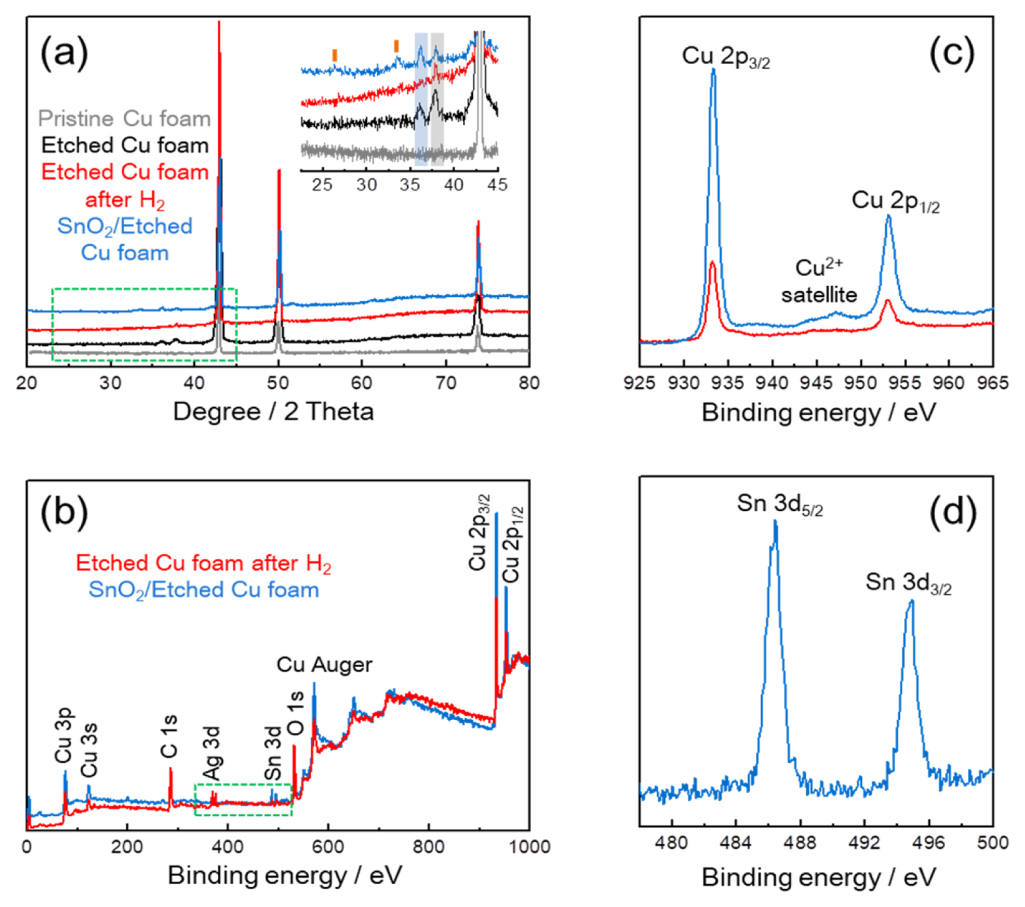
Fig. 3a shows the XRD patterns of Cu foams at different states; pristine, etching, H2 reduction, and SnO2 coating processes. Only metallic Cu (JCPDS 04-0836) phase is observed in the Pristine Cu foam, while CuO (JCPDS 45-0937; as indicated by blue box) and Ag (JCPDS 04-0783; as indicated by black box) phases are additionally confirmed in the Etched Cu foam, which implies that the partial oxidation of Cu foam and the Ag deposition are accompanied during the etching process. After that, the absence of CuO in Etched Cu foam after H2 shows a result of the effective reduction of CuO into metallic Cu. SnO2 (JCPDS 41-1445; as indicated by orange bar) phase is identified in the SnO2/Etched Cu foam [11], and meanwhile the re-appearance of CuO indicates that the partial oxidation of Cu foam occurs again during the SnO2 sol-gel coating process. XPS analysis was used for the determination of chemical environment and oxidation state of copper. Including the Ag in Etched Cu foam after H2, Sn is observed from a survey spectrum of the SnO2/Etched Cu foam in Fig. 3b as indicated by green dot box. Compared to the Etched Cu foam after H2, the shake-up satellite of SnO2/Etched Cu foam in the 2p Cu spectrum (Fig. 3c) confirms the existence of Cu2+ on the surface of SnO2-coated Cu foam, in accordance with the partial re-oxidation during the SnO2 coating process (Fig. 3a) [11,18–20]. In Sn 3d spectrum of the SnO2/Etched Cu foam (Fig. 3d), 8.4 eV of separation distance between Sn 3d5/2 and Sn 3d3/2 identifies a formation of Sn4+ oxidation state in the SnO2 coating layer [21,22].

(a) XRD patterns of Cu foam after pristine, etched, reduced under H2 and SnO2-coated states, and XPS (b) survey and (c) Cu 2p spectra of reduced Cu foam and SnO2-coated Cu foam, and (d) Sn 3d spectrum of SnO2-coated Cu foam.
To confirm electrochemical reactions depending on the H2 reduction process in the Etched Cu foam, cyclic voltammetry (CV) measurement was conducted in voltage range of 0.01–3 V at a scan rate of 0.1 mV s−1 (Fig. 4a). For the Etched Cu foam, the first CV curve, composed of the initial reduction peak at ~1.1 V and subsequent reduction peak at ~0.8 V upon cathodic scan process, and the oxidation peak at ~2.5 V upon anionic scan process as indicated by the blue box, can be a representative of the electrochemical behaviors of CuO [16,23]. The distinct redox peaks are observed in the Etched Cu foam, whereas no apparent peaks are identified in the Etched Cu foam after H2, demonstrating the reduced CuO phase after the hydrogen heat-treatment. Additionally, the noticeable peak at ~0.3 V upon anodic scan process can be related to de-alloying reaction of Ag-Li, which support the existence of Ag again in the Cu foam [24]. The first five CV curves of the SnO2/ Etched Cu foam (Fig. 4b) are in accord with the electrochemical behaviors of the SnO2-based materials [5,25–27]. During the first cycle, the cathodic peak at ~0.75 V is attributed to the irreversible formation of solid electrolyte interface (SEI) layer by electrolyte decomposition, and the reduction of SnO2 to Sn by conversion reaction. The cathodic peak under ~0.5 V is indicative of alloying reaction for forming Sn-Li, and the corresponding anodic peak until ~1.0 V is due to de-alloying reaction of the Sn-Li alloy. Furthermore, the cathodic peak ~1.1 V as indicated by the blue box can corresponds to the reduction of CuO, which also accords with the re-appearance of CuO phase (Fig. 3a) after the SnO2 coating process.

Cyclic voltammetry of (a) etched and reduced Cu foams during the first cycle, and (b) SnO2-coated Cu foam during the first five cycles.
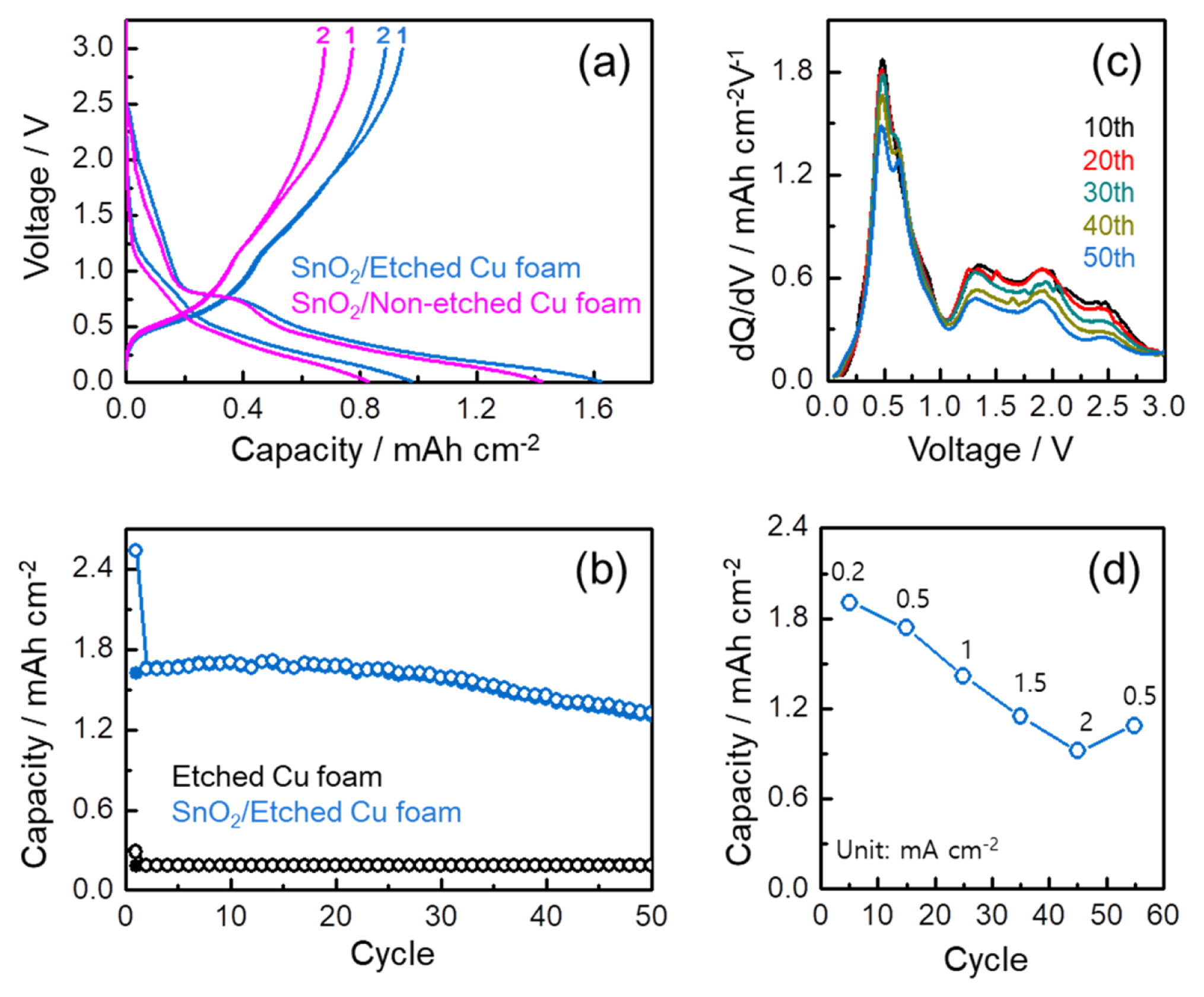
Despite an importance of the evaluation on gravimetric capacity, by the co-existence of the Ag, CuO, and SnO2 phases all reacting toward the lithium, and the difficulty in measuring accurately the mass of each active material in the SnO2/Etched Cu foam, the electrode performance in this study was evaluated per area as shown in Fig. 5. To confirm the effect of etched Cu foam substrate on the areal capacity, galvanostatic discharge and charge profiles of the SnO2/ Etched Cu foam and SnO2/Non-etched Cu foam were compared (Fig. 5a) wherein the SnO2/Non-etched Cu foam is the electrode using the pristine Cu foam in absence of the etching process. Along with the higher capacity retention, the higher discharge and charge capacities are achieved in the SnO2/Etched Cu foam, which can be a result of the higher SnO2 loading in the etched Cu foam with the internal utilization through the surface pore. Fig. 5b indicates the cycling performance of the SnO2/Etched Cu foam for 50 cycles. At the same time, the cycling performance of the Etched Cu form including the developed CuO phase was also evaluated to confirm the contribution of the CuO into the areal capacity of the SnO2/Etched Cu foam. It can be estimated that maximum ~11% for the first charge capacity of ~1.6 mAh cm−2 is originated from the CuO phase in the SnO2/Etched Cu foam. Moreover, the high lithium storage of 1.3 mAh cm−2 after 50 cycles is fairly comparable to the reported Sn-based anode materials [28–31]. From the comparison of the differential capacity profiles (dQ/ dV vs. voltage) at the selected cycles upon charge process in Fig. 5c, the stable capacity retention of the SnO2/Etched Cu foam is resulted from the reversible de-alloying reaction of the Sn-Li alloy in spite of the decrease in the re-oxidation reaction of Sn into SnOx upon cycling [5,6,11,32]. The rate capability of the SnO2/Etched Cu foam was evaluated by increasing stepwise the current rate from 0.2 to 2 mA cm−2, and then decreasing back to 0.5 mA cm−2, as shown in Fig. 5d. Each rate step consists of 10 cycles and the capacity in Fig. 5d corresponds to the capacity at the 5th cycle. Compared to ~1.9 mAh cm−2 at 0.2 mA cm−2, ~0.9 mAh cm−2 is obtained even at 2 mA cm−2. When the current rate is reduced back to 0.5 mA cm−2 after 50 cycles, the SnO2/Etched Cu foam recovers a respectable amount of the capacity, demonstrating its good rate capability.

(a) The first two voltage profiles of SnO2-coated Cu foams with and without etching process at 1.7 mA cm−2, (b) cycle performance of etched Cu foam and SnO2-coated Cu foam at 0.5 mA cm−2 for 50 cycles, (c) dQ/dV profiles of SnO2 -coated Cu foam at the selected cycles upon charge process, and (d) rate performance of SnO2-coated Cu foam at various current rates.
4. Conclusions
The 3D etched Cu foam was prepared through the auto-catalytic electroless plating method wherein the dissolution of copper metal into Cu2+ and the deposition of silver ion into Ag occur spontaneously, and it was used as the current collector for electron path and the substrate for SnO2 coating at the same time to obtain the integrated electrode. After that, the SnO2/ Etched Cu foam was fabricated by the sol-gel coating process, and directly applied to LIBs anode. The newly-formed secondary pores resulted from the catalytic dissolution of Cu metal, of both several micrometers and several tens of micrometers, extended the utilization on the surface area of Cu foam by penetrating the individual strut of Cu foam. Consequently, the surface area for SnO2 loading was increased with the internal utilization through the additional surface pore, and the increased areal capacity with high structural integrity during cycling was also demonstrated compared to the SnO2/Nonetched Cu foam, which enables the non-galvanic electroless method to have the potential for the surface modification on various metal substrates.
Acknowledgement
This research was supported by a National Research Foundation of Korea (NRF) grant funded by the Korean government (MSIP) (No. NRF-2017R1A4A1015770). This work was supported by the National Research Foundation of Korea(NRF) grant funded by the Korea government(MSIT) (No. NRF-2019R1A2C1003499). This research was supported by Basic Science Research Program through the National Research Foundation of Korea(NRF) funded by the Ministry of Education(NRF-2016R1A6A3A11932369).
