3D Printed Flexible Cathode Based on Cu-EDTA that Prepared by Molecular Precursor Method and Microwave Processing for Electrochemical Machining
Article information
Abstract
In this work, a metal-ligand solution (Cu-EDTA) was prepared based on the molecular precursor method and the solution was spin-coated onto 3D printed flexible photosensitive resin sheets. After being processed by microwave, a laser with a wavelength of 355 nm was utilized to scan the spin-coated sheets and then the sheets were immersed in an electroless copper plating solution to deposit copper wires. With the help of microwave processing, the adhesion between copper wires and substrate was improved which should result from the increase of roughness, decrease of contact angle and the consistent orientation of coated film according to the results of 3D profilometer and SEM. XPS results showed that copper seeds formed after laser scanning. Using the 3D printed flexible sheets as cathode and galvanized iron as anode, electrochemical machining was conducted.
1. Introduction
LPKF Group which is a leading supplier of laser-based solutions for the technology industry developed a laser-supported process for producing three-dimensional MIDs (molded interconnect devices) named as LPKF-LDS (LPKF-Laser Direct Structuring) in 1997 [1,2]. Since then, LPKF-LDS has attracted much attention and been widely used in the industry due to its advantages such as 1) circuit layouts which can be created on metal-ligand 3D parts without using cables or separate circuit boards, 2) low manual stress on the hands and 3) reduced weight and dimensions of the 3D circuits [3,4]. Considering these advantages, the application of LPKF-LDS in fabricating flexible cathode for electrochemical machining (FCEM) was expected [5,6]. Electrochemical machining using flexible cathode can make the preparation of textures on freeform surfaces easier than the traditional processes and can effectively reduce the time and costs for the reusability of flexible cathode. Based on the process of LPKF-LDS, previously, reducing agent was mixed into the polymer and worked as a catalyst in the electroless copper plating process after being scanned by laser [7]. However, the bubbles are unable to be eliminated in the preparing process of the polymer sheets, leading to a negative impact in adjusting the accuracy of the plated copper wires, and the mechanical properties such as flexibility and brittleness would also degrade. On the other hand, for LPKF-LDS, only a thin layer of the sheets needs to be activated by laser, reducing agent is not necessary to be introduced into the layers that under the activated layer [8–11]. All the problems make the thin film coating process as an ideal choice for preparing flexible cathode for electrochemical machining. However, the adhesion between thin film and substrate is usually not good and need to be optimized. To solve this issue corona [12], plasma [13], alkali [14] and amine treatment [15], etc. have been used to improve the adhesion and showed good results, but causing environmental problems and uni-deal efficiency limited their practical applications.
In this paper, as shown in Fig. 1, a wet chemical process, Molecular Precursor Method (MPM) [16–19], is used to fabricate thin films on 3D printed flexible cathode to get Flow Channel and Electrode Integrated Cathode (FCEIC). Microwave processing is introduced to modify the surface of 3D printed flexible sheets, adjust the concentration of MPM solution and dry the coated flexible sheets. The thin film coated sheets are scanned by a laser with a wave-length of 355 nm and then are immersed into the electroless copper plating solution. Using the 3D printed flexible sheets as cathode and galvanized iron as anode, electrochemical machining is conducted.

Preparing process of 3DP flexible cathode.
2. Experimental
2.1 Preparation of Cu-EDTA Solution
11.7 g ethylene diamine tetraacetic acid (EDTA, 99%, Aladdin) and 8.0 g copper acetate monohydrate (Cu(CH3COO)2?H2O, 99%, Aladdin) were dissolved into 300 ml 75? deionized water and stirred for 6 hours using a magnetic stirrer (ZNCL-B, Gongyi Yihua Instrument Co., Ltd). After leaching and evaporation, Cu-EDTA powder was obtained. According to the molar ratio of 1:2 of Cu-EDTA: dibutylamine (99%, Aladdin) and the concentration of copper ion in the solution as much as 0.7 mmol/g, 4.32 g Cu-EDTA and 3.15 g dibutylamine were dissolved into 10 g ethanol and refluxed at 75°C for 1 hour. The obtained solution was then radiated by microwave for 5 minutes to get a honey-like gel.
2.2 Fabrication of Thin Films
Spin-coating was used to prepare thin films on 3D printed sheets that was fabricated by a Stereo Lithography Appearance machine (SLA, RS-350S) based on a kind of flexible photosensitive resin. The size of 3D printed sheets was 20×50 mm2. 3 mL of microwave processed solution was dropped onto the 3D printed sheets at 500 rpm for 5s and then the rotation speed of the spin coater was increased to 5000 rpm. After 60 seconds’ spin-coating, the coated 3D printed sheets were transferred to an oven to be dried at 70°C for 60 mins followed by transferring into a microwave oven to be radiated for 2 minutes. And the thickness of the thin film obtained was about 120 μm.
2.3 Laser Activation of 3D printed flexible sheets
A laser (FOTIA-355-5W-50K, INNO LASER, China) with a wavelength of 355 nm was used to scan the 3D printed and thin film coated flexible sheets. The laser scanning process parameters were as follows: spot mode TEM00, spot diameter 15 μm, scanning speed 30 mm/s, average power 0.8 W, repetition rate 150 KHz.
2.4 Electroless Copper Plating
The laser scanned substrates were rinsed with deionized water and then immersed into the electroless copper plating solution at 50°C for 2 h and then rinsed with deionized water. The electroless copper plating solution was prepared as follow. Firstly, 1.6 g copper sulfate was fully dissolved in 25 mL of deionized water, and then metal-liganding agents that consist of 1.4 g C4O6H4KNa and 2.5 g EDTA-2Na were added to the copper sulfate solution to form a metal-ligand of copper ions. Secondly, a sodium hydroxide solution that consist of 1.4 g sodium hydroxide and 25 mL deionized water was added to the copper sulfate solution. Finally, the stabilizer (0.8 mg 2,2′-Bipyridyl and 7 mg K4Fe(CN)6·3H2O), reductant (1.2 mL HCHO) and deionized water were added to obtain 100 mL electroless copper plating solution.
2.5 Electrochemical Machining
Using the Cu-EDTA coated 3DP sheets as cathode, 5% sodium nitrate solution (with deionized water as solvent) as electrolyte and galvanized iron sheet as anode, electrochemical machining was carried out. Based on a lot of experimental results, optimized processing parameters were confirmed as voltage 15 V, pulse frequency 15 kHz and duty cycle 50%.
2.6 Characterizations
3D profilometer (KEYENCE Inc. VR-5100) was used to measure the roughness of the substrate. The contact angle of the substrate was measured by Itd JC2000DX (Shanghai zhongchen Co.). Surface morphologies of plated coatings were observed using a built-in spectrometer benchtop Scanning Electron Microscope (SEM, ZEISS Sigma 500). X-ray Photoelectron Spectroscopy (XPS, Thermo escalab 250Xi) and X-ray Auger Electron Spectroscopy (XAES) were used to characterize the valence of copper before and after laser scanning. Before XPS characterization, the surface of the sample was etched with an Ar ion beam with an etching depth of 5 nm to eliminate the effect of surface contamination. Depth profiles were obtained based on an etching rate of 20 nm/100 s. Adhesion between plated copper wires and substrate was measured with the scotch tape that was produced by 3M according to ASTM-D3359-09. The electrochemical machined parts were also characterized by 3D profilometer (KEYENCE Inc., VR-5100).
3. Results and Discussion
For the high surface energy of photosensitive resin, solutions cannot be evenly spin-coated directly. In order to eliminate the aggregation of spin-coated solution, before spin coating, the 3DP parts and MPM solutions were respectively radiated by microwave for 5 min. For the photosensitive resin, after microwave processing, as shown in Table 1, the decrease of Sa, Sz and Str indicated that the surface texture becomes more regular after microwave processing, the increase of Spc and Sdr indicated that the surface texture becomes sharper and the area becomes bigger after microwave processing which is benefit for improving the adhesion. Fig. 2a and Fig. 2b show the contact angle of 3DP parts after microwave. The contact angle decreased from 46° to 33° indicating that 3DP parts became more hydrophilic after being radiated by microwave. In a word, after being radiated by microwave for 5 minutes, the roughness and hydrophilic of the 3D printed flexible photosensitive resin increased and the concentration of the MPM solution increased, and thus MPM solution can be evenly spin coated onto the surface of the 3DP parts.
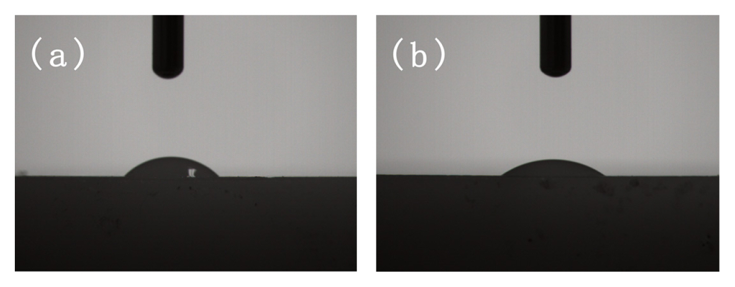
Contact angle of 3DP parts a) before microwave and b) after microwave.
After spin coating, the substrates were radiated by microwave again. Fig. 3 (a) and (b) compare the morphologies of the substrates before and after microwave processing. Before microwave processing, the voids and crevice can be observed and the orientation of the particle was inhomogeneous. After being processed by microwave, the orientation of the particles became homogeneous and grown in the same direction, and compact films were obtained. The change of the orientation of the particles should result from the structure and polarity of Cu-EDTA which is shown in Fig. 4.
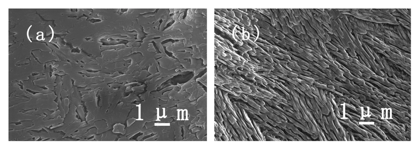
Surface morphologies of a) before microwave processing and b) after microwave processing.

A perspective drawing of Cu(H2edta)(H2O).
Since Cu-EDTA consisted of EDTA and Cu ion where EDTA (ethylenediaminetetracetic acid) acts as a universal chelate agent providing two nitrogen atoms and four carboxyl oxygen to a metal ion, a chelation occurred between EDTA and copper ion leading to product Cu-EDTA as shown in Fig. 4 [20]. The dihydrogen ethylenediaminetetra-acetate ion (H2edta) acted as a quinquedentate ligand, one acetate group remained free, and the six-co-ordination of the copper was accomplished by a water molecule. A distorted octahedron structure of Cu-EDTA consists of four coplanar bonds and two tetragonal bonds. Due to the unsymmetrical structure and an exposed carboxyl group, Cu-EDTA performed as a polar molecule. When the polar molecules Cu-EDTA were exposed to microwave, the orientation of the polar molecules would change with the microwave electromagnetic field, and thus the orientation of the polar molecules would change from random to orderly which was consistent with the SEM results.
Laser-induced chemical process consists of two kinds of reactions as thermal and photochemical reaction while photochemical reaction is the main process. The primary reaction in the laser-induced chemical process includes the rupture of molecular bonds. During laser scanning, the chelating bonds in the molecule were broken down. If the dissociation energy of each molecule was caused by a photon, and the dissociation energy required for each mole of molecules was equal to the energy of 1 mole of photons, then the dissociation energy D0 of 1 mole of molecules can be got according to D0=1.1963×10⁵/λ. Therefore, in the process, since the corresponding dissociation energy of the ultraviolet laser was about 337.0 kJ/mol which was bigger than the coordination bond between EDTA and Cu2+, the photo dissociation reaction occurred. The specific photo dissociation process can be roughly divided into two steps. Fig. 5(c) showed the diagram of the reaction, firstly, an excitation occurred in the binding orbital with a minimum energy, then the excited particles migrated to the relatively stable anti-bonding orbital after separation and resulted in the bond fracture.
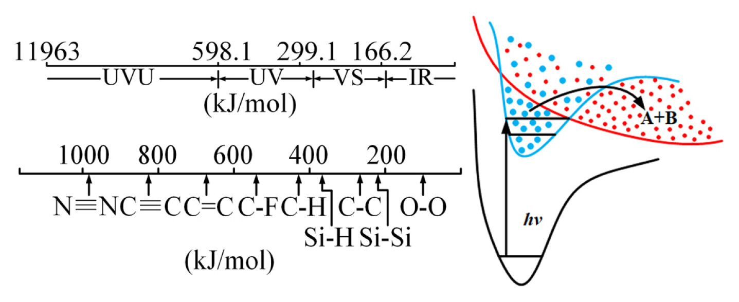
Schematic diagram of binding energy and laser energy.
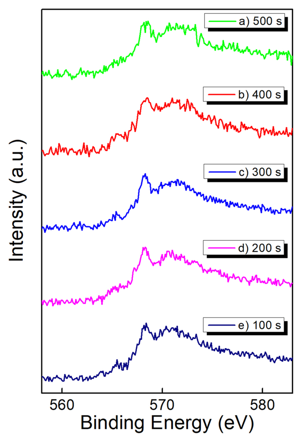
In order to reveal the copper plating mechanism of the flexible cathode with Cu-EDTA, laser activation areas were characterized by XPS and the results are shown in Fig. 6. As shown in Fig. 6f, before scanning, the thin film exhibited a Cu 2 p3/2 peak and Cu 2 p3/2 at a binding energy of 934.4 eV and 953.9 eV, together with intense satellite peaks at 938.9 eV and 943.7eV, these two peaks overlapping, and 962.4 eV which completely corresponded to the standard XPS spectrum of CuO phase [21,22]. Fig. 5 (a)–(e) show the XPS spectra of Cu 2p in the thin film at 100 s, 200 s, 300 s, 400 s and 500 s of etching time. The positions of the Cu 2 p3/2 and Cu 2 p1/2 in different depth as shown in Fig. 6 (a)–(e) were respectively 932.5 eV, 932.5 eV, 932.6 eV, 932.6 eV, 932.5 eV and 952.5 eV, 952.5 eV. 952.5 eV. 952.5 eV, 952.6 eV which indicated that the valence states of copper ions were consistent at different depths in the activated region.

XPS spectra of Cu 2p in the thin film using Al-Kα X-ray (hv=1486.6 eV).
The shape of Cu0 and Cu+ peaks were similar to each other and it was difficult to distinguish them. To identify the specific valence of copper, the laser scanned sheets were further characterized by XAES. As shown in Fig. 7, two main peaks were obtained in the laser area. The peaks of each spectrum were slightly different, and the energies of the peaks were in a range of 568.28–568.38 eV and 571.18–571.48 eV, respectively. Referring to auger spectral database, it can be inferred that copper existed in a form as Cu+ with relatively little Cu metal being formed in the laser scanned area [23,24]. Therefore, it can be confirmed that the chemical bonds between EDTA and Cu were broken down by laser, and the resultant Cu+ acted as a catalytic core in the electroless copper plating.
Auger electron spectra of Cu LMM in the thin film.
Fig. 8 shows the adhesion measuring results of the copper film. According to the norm ASTM-D3359-09, the adhesion could be divided into six levels. By comparing with the standard card, the adhesion of the copper film can be identified. Before microwave processing (Fig. 8b) the adhesion of copper film can be identified as level 2B while after microwave processing the copper film (Fig. 8b) can be identified as level 4B. This indicated that microwave processing can improve the adhesion between copper wires and substrate. Considering the results of SEM and contact angle, the improvement of adhesion should result from the increase of roughness, decrease of contact angle and the consistent orientation of coated film.
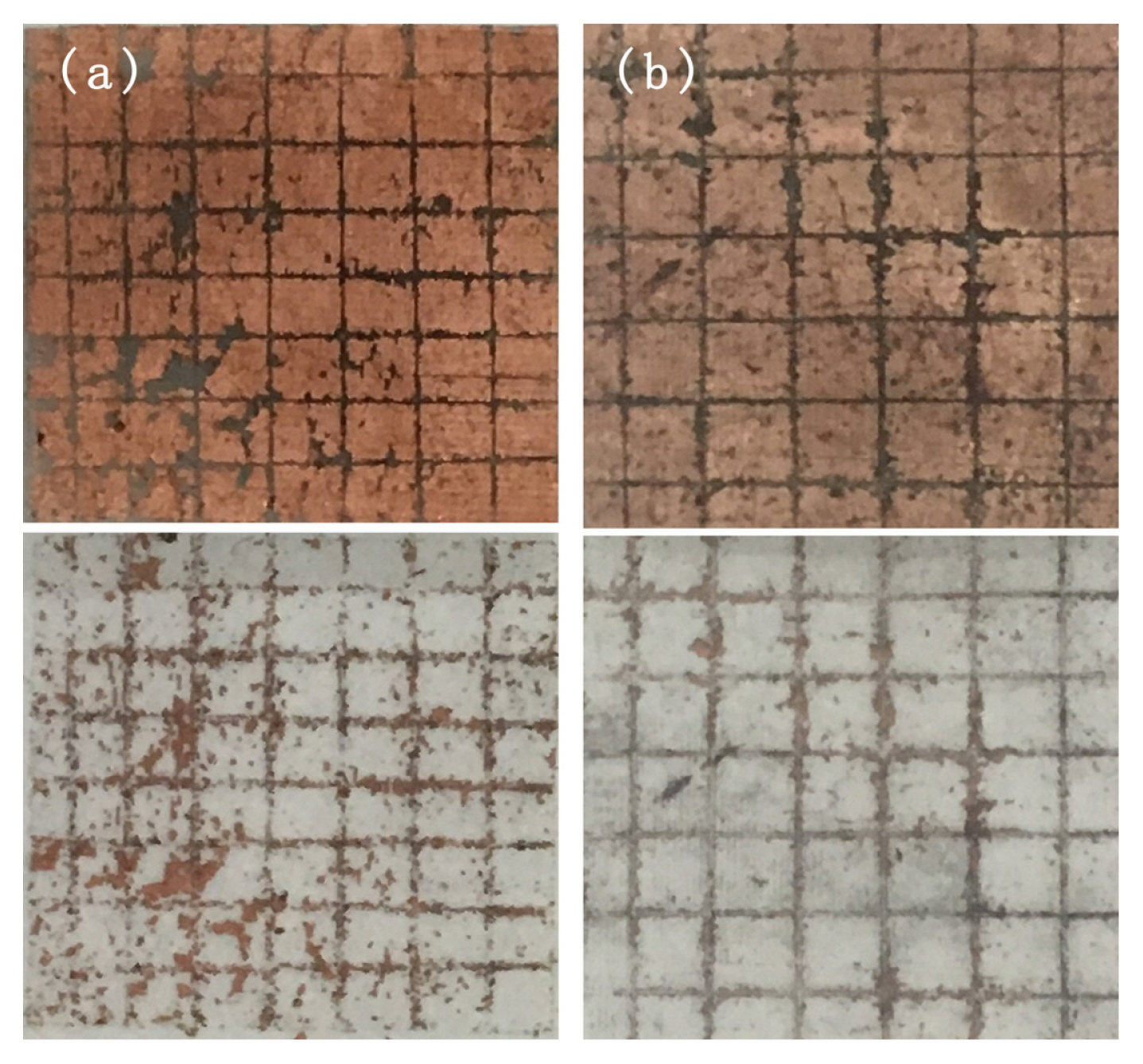
Adhesion measuring results of copper film with average power of 0.8W, repetition rate of 150 KHz and scanning speed of 30 mm/s a) before microwave processing and b) after microwave processing.
Based on the flexible cathode, using sodium nitrate (NaNO3) as the electrolyte and galvanized iron sheet as the anode, electrochemical machining was carried out. For electrochemical machining, as is known, interelectrode gap and current density are the main influencing factors for machining accuracy. Interelectrode gap should be as small as possible and current density should be stable to get good machining accuracy. Usually, when the interelectrode gap is constant, in order to get good machining accuracy, the current density should be big and stable which indicated that the voltage and pulse frequency should be high, and duty cycle should be small. Based on the regular patterns and optimization of processing parameters, 15 V voltage, 15 kHz pulse frequency and 50% duty cycle were used to conduct electrochemical machining and the results were shown in Fig. 9. It can be found that a clear line with a width of ~110 μm was obtained on the galvanized iron sheet.
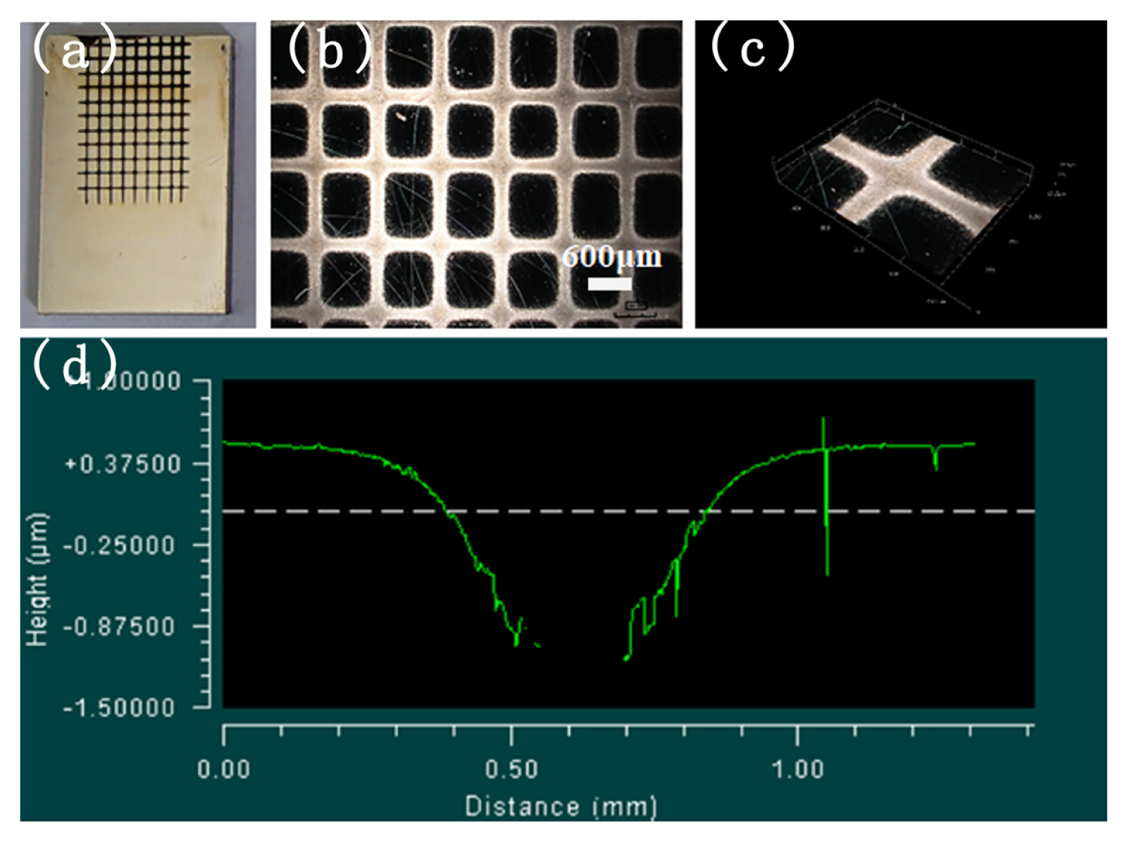
Electrochemical machining sample based on flexible cathode consist of Cu-EDTA coated substrate.
4. Conclusions
Based on the molecular precursor method, Cu-EDTA was spin coated onto 3D printed flexible photosensitive resin substrates and then been scanned by ultraviolet laser. The activated Cu-EDTA films provided fine copper plating seeds for electroless copper plating process. Microwave processing was introduced into the preparing process. By the help of microwave processing, the surface roughness of substrates increased, the contact angle of substrates decreased and the orientation of coated film became consistent, and thus the adhesion between copper wires and substrates was improved. Electrochemical machining was carried out using the 3D printed flexible sheets as cathode and galvanized iron as anode. This process provided a simple and cost-effective alternative way to prepare flexible cathode for electrochemical machining and showed some advantages on improving the precision of electrochemical machining for the uniform distribution of gap and consistent distribution of small gap flow field by the help of FCEIC.
Acknowledgment
This work was supported by National Natural Science Foundation of China (51475174), Natural Science Foundation of Fujian Province (2017J01089), Scientific Research Funds of Huaqiao University (Z16Y0020) and Subsidized Project for Postgraduates’ Innovative Fund in Scientific Research of Huaqiao University.