1. Introduction
Because of its variable oxidation states, Nb, a transition metal, can react with various elements such as oxygen, carbon, and nitrogen to form a wide range of functional compounds. One such compound is Nb
2O
5, which has received significant attention as an electrode material for sensors [
1ŌĆō
4], dye-sensitized solar cells [
5], photodetectors [
6], and capacitors [
7,
8], because of its large band-gap (3.2~4 eV) [
9] and high dielectric constant (~41) [
10]. Moreover, it can be applied as an electrode material in lithium secondary batteries because of its excellent energy storage per unit volume as well as its suitable charge and discharge potentials [
11,
12].
Porous materials are known to have numerous benefits, particularly when used as electrodes in functional electrochemical devices. Because of their large surface areas [
13ŌĆō
16], these electrodes often show improved capacitance, extraordinary sensitivity, and increased power when used in capacitors [
17,
18], sensors [
19], and secondary batteries, respectively [
20,
21]. In addition, the low fill factor, i.e., the large free volume of porous materials, facilitates the rapid movement of ions/atoms through the material, possibly suppressing the concentration overpotential [
13,
21]. Thus, the efficiency of the devices is significantly improved, particularly when mass transport is the rate-determining process [
14]. A large free volume can also enhance the durability of the device by serving as a buffer against the possible expansion or contraction of the material during operation [
14,
22,
23].
Various wet-chemical methods such as hydrothermal synthesis, solŌĆōgel processing, anodic oxidation, and chemical/electrochemical etching have been used for the preparation of porous materials. Among these, the electrochemical methods are cost-effective, as they involve simple device configuration and easy control of the process variables (i.e., current and voltage). In addition, they aid in obtaining highly reproducible results. Thus, the electrochemical fabrication of a wide range of porous materials has been extensively studied. Porous Nb structures have been obtained via the anodic oxidation of Nb [
24ŌĆō
26]. However, this process either requires the use of a toxic chemical, HF, in an aqueous solution [
27] or high-temperature conditions (>160┬░ C) in a non-aqueous solution [
28]. Additionally, the product is limited to a porous Nb oxide. Electrochemical etching is another well-known and cost-effective method that can be used to prepare a porous Nb structure [
7,
29]. However, HF is also commonly used in this process, although it has been reported that an appropriate combination of HF with different types of organic solvents can allow for good control over the formation of the porous Nb surface [
29].
In this study, a porous Nb structure was prepared via a one-pot, HF-free, electrochemical etching process. In particular, a novel hierarchical porous Nb or self-similar fractal porous Nb structure was successfully obtained using the pulse etching. Initially, the effect of the applied current density on the uniformity and density of the pores was examined. Subsequently, critical factors, namely, the type of etching process (continuous vs. pulse) and the etchant concentration, affecting the hierarchical order of the pores were optimized. In addition, the surface area of the porous structure was theoretically evaluated as a function of the hierarchical pore order. The actual pore shape and hierarchical pore order were examined on the basis of this theoretical study and the obtained experimental results.
3. Results and Discussion
Fig. 1 shows the morphology of the porous Nb surfaces etched in a methanolic solution of 1 M H
2SO
4 for 10 min at anodic current densities ranging from 30 to 100 mA cm
ŌłÆ2. The application of a low current density, 30 mA cm
ŌłÆ2, led to the formation of a low-density porous structure, wherein pores were formed only on selected regions of the surface (
Fig. 1a, b). Increasing the current density to 50 mA cm
ŌłÆ2 created a relatively uniform porous structure with pore diameters of approximately 25 ╬╝m (
Fig. 1c, d); however, a further increase in the current density to 100 mA cm
ŌłÆ2 resulted in excessive etching with severe overlap among the pores (
Fig. 1e, f).
Pore formation during electrochemical etching progresses via pore nucleation and subsequent pore growth. Notably, the aggressive anions in the etching solution preferentially interact with the energetically activated local domains to induce pore nucleation. In many previous studies on electrochemical etching using etchants containing HF or F
ŌłÆ, highly localized dissolution of the metal surface was observed, which resulted in the formation of pores with small diameters and high aspect ratios [
30,
31]. However, despite their utility in the formation of porous structures with large surface areas, the use of chemicals containing F
ŌłÆ ions should be avoided because they are hazardous to the environment. Therefore, in this study, H
2SO
4 was used as the etchant and the SO
42ŌłÆ ions behaved as the aggressive anions. It was hypothesized that the relatively low aggressiveness of SO
42ŌłÆ compared to that of F
ŌłÆ would result in the formation of pores with larger diameters, as the regions of dissolution on the metal surface would be broader when SO
42ŌłÆ is used. The experimental results were found to be in good accordance with this hypothesis (
Fig. 1). Pore nucleation and growth induced by SO
42ŌłÆ might occur via a mechanism similar to that of localized corrosion, as follows: (1) localized destruction of the passivation film on the metal surface by SO
42 ; (2) electrochemical oxidation (dissolution) of the metal and subsequent pore nucleation; (3-1) entry of SO
42ŌłÆ into the pores due to its electrostatic attraction to the dissolved metal cations; (3-2) formation of metal sulfate, followed its hydrolysis to produce the metal hydroxide and sulfuric acid, thus increasing the acidity of the pores; (4) pore wall dissolution (pore growth) due to the increased acidity and SO
42ŌłÆ concentration.
Thus, it is apparent that during pore formation, the pore growth rate is significantly affected by the concentrations of the SO42ŌłÆ and H+ ions inside the pores, which are influenced by the concentration of the metal cations inside the pores. The duration for which the dissolved metal cations remain in the pores depends on the effective porosity of the pores. If the pores have a relatively closed conformation, then it is challenging for the metal cations to diffuse out, thus promoting the inflow of anions and pore growth. In contrast, open pores facilitate the diffusion of the metal cations, thus suppressing the inflow of anions and preventing pore growth. The pores formed in this study seemed to have an open conformation, indicating that the concentration of the dissolved Nb ions in the pores was low during electrochemical etching. This hindered the pore growth and suggested that optimizing the etching conditions could result in the formation of remarkably small pores with compact structures.
Current density provides the electrochemical driving force for pore formation, making it a critical factor to consider for the controlled growth of the pore structure. However, from the numerous experiments performed under various conditions, it was observed that the continuous application of a constant current density alone could not result in the formation of an ideal porous structure, i.e., a rough Nb surface with large specific surface area. Small-diameter, low-density pores were formed at a low current density (30 mA cm
ŌłÆ2 ) while large-diameter, severely overlapped pores were obtained at a high current density (100 mA cm
ŌłÆ2 ), as shown in
Fig. 1. Therefore, the optimized current density was chosen to be 50 mA cm
ŌłÆ2, so that a relatively compact and uniform pore structure was formed. Other factors affecting the specific surface area of the pore structures were subsequently optimized at this current density.
The open conformation of the pores is generally stable and difficult to modify. Thus, the open pores formed by the application of the optimized current density (henceforth referred to as the primary pores) can be considered to be the framework for the formation of a hierarchical porous structure, which can significantly increase the specific surface area of the porous material. The open conformation of the pores and pore nucleation results from the interaction of the aggressive ion, SO42ŌłÆ, with the activated local domains. However, the concentration of SO42ŌłÆ inside the pores is substantially low due to the difficulty in the migration of these ions into the open pores. Moreover, even if diffusion did occur, it is unlikely that the shortage of SO42ŌłÆ ions would be relieved, as the electrochemical Nb etching is thought to follow the typical diffusion-controlled mechanism.
Thus, it is assumed that electrochemical etching under a continuous application of current would lead to the formation of primary pores only. Therefore, to obtain a hierarchical porous structure, the high SO42ŌłÆ concentration must be maintained throughout the etching process in order to continuously induce pore nucleation, and thus, pore growth on the porous surface. This can be achieved by the pulse etching method, which facilitates the supply of the reactants to the pore surface during the rest time between etching processes. Thus, a high SO42ŌłÆ concentration is reestablished, and pore nucleation is successfully induced during the subsequent re-etching process.
Figs. 2a and b show the surface morphology of Nb obtained via the pulse etching process, which involved the application of a 50 mA cm
ŌłÆ2 current density for 10 min, followed by a 1 min rest time, and then, an additional 5 min application of the 50 mA cm
ŌłÆ2 current density in a methanolic solution of 1 M H
2SO
4. Interestingly, the formation of small pores (secondary pores) on the walls of the large pores (primary pores) could be observed even after the first pulse cycle, i.e., one repetition of ŌĆśthe rest time followed by an additional 5 min current applicationŌĆÖ. This observation strongly supports the hypothesis stated earlier; hierarchical pores can be formed through the pulse etching of Nb performed at the optimized conditions. Low-density secondary pores were formed after the application of the first pulse cycle, possibly due to the rapid consumption of the additional SO
42ŌłÆ ions that were supplied during the rest time. Thus, the number of pulse cycles was increased to examine the pattern formation of the small pores.
Figs. 2c and d show the surface morphology of the porous Nb obtained from ten pulse cycles. High-density secondary pores with diameters of approximately < 1 ╬╝m were successfully created with negligible overlap between the secondary pores. However, after 300 pulse cycles, the uniformity of the pores drastically degraded (
Fig. 2e, f), and insignificant amounts of high-order hierarchical pores were created. This implies that increasing the number of pulse cycles when the concentration of SO
42ŌłÆ is 1 M leads to over-etching of the low-order (i.e., primary and secondary) pores, thus causing the overall framework of the porous structure to collapse. In addition, increasing the number of pulse cycles does not facilitate the nucleation of high-order pores with much smaller sizes.
Therefore, in order to achieve a well-defined, high-order hierarchical porous structure, the nucleation of high-order pores needs to be promoted while the over-etching of low-order pores should be prevented during the etching process. Thus, the initial SO
42ŌłÆ concentration was increased to allow the pulse etching to proceed in a more aggressive etching environment, and the experiment was performed only till 10 pulse cycles.
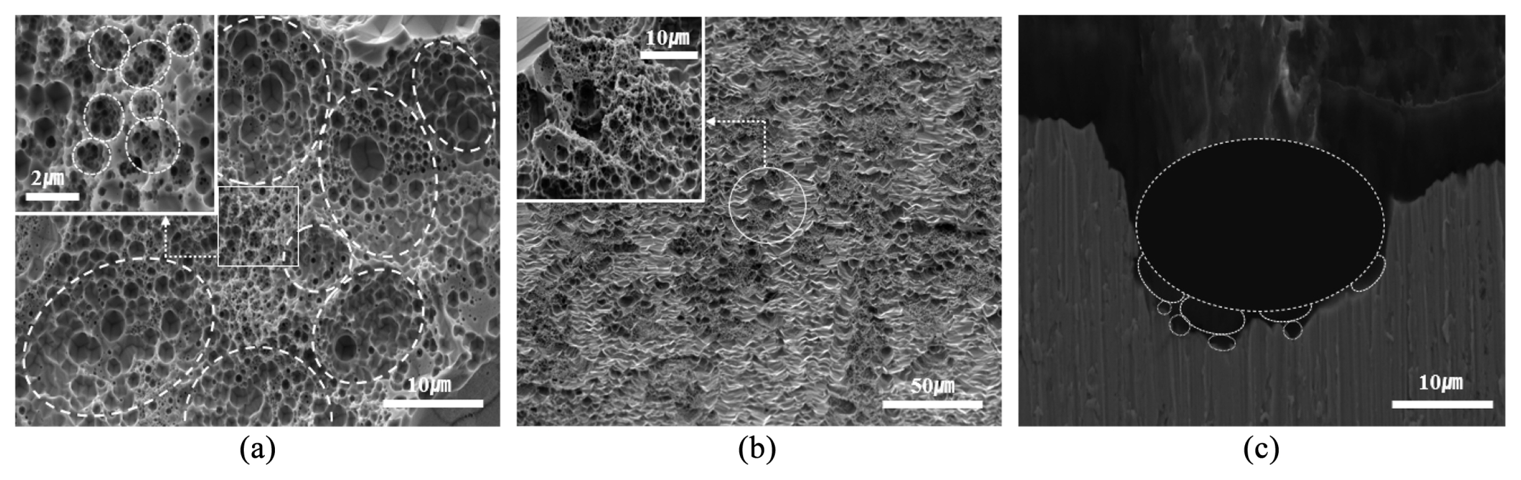
Figs. 3a, b and c show the surface, inclined, and cross-sectional images of the porous Nb structure obtained from 10 repetitions of pulse etching in a methanolic solution of 1.5 M H
2SO
4. Surprisingly, simply increasing the SO
42ŌłÆ concentration during pulse etching led to the formation of homogeneous, hierarchical pore structures. The formation of tertiary pores was verified through electron microscopy, although higher order pore structures may have also been created. Although this hierarchical pore structure involves rather limited iteration, it can be viewed as a fractal porous structure with self-similarity.
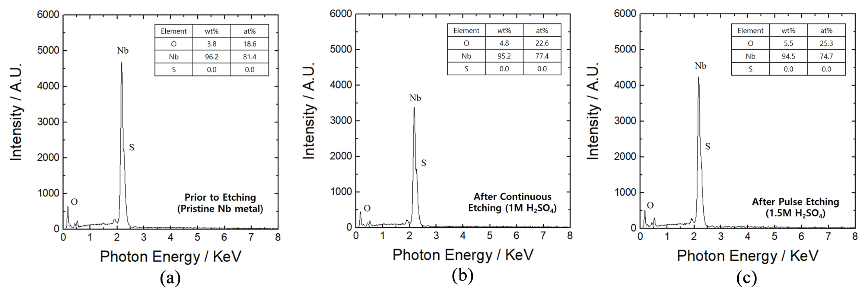
It is further noted that the surface composition of the porous Nb samples, obtained from continuous and pulse etching, was almost the same as that of the pristine Nb metal (i.e., the sample prior to etching), as shown in
Fig. 4. This strongly indicates any oxides or sulfates were not formed on the Nb surface during the etching process. Oxygen detected both on the pristine and etched Nb samples might originate from the native oxide layer spontaneously formed when they were exposed to the atmosphere.
This study also proposes a theoretical approach for the in-depth analysis of the surface area as a function of the hierarchical order of pores. The overall surface area of a flat porous material can be expressed as follows:
where
n represents the hierarchical order of the pore structure.
Stotal,n,
Sporous,n, and
Snon-porous,n represent the total surface areas of the porous material, pores, and free material, i.e., the area of the material without pores, respectively. Geometrically, when a 2D surface is densely packed with a hexagonal arrangement of circles, the circles occupy approximately 90.7% of the surface, regardless of their diameter, leaving a free area of 9.3%. This concept was used to simplify the calculations; it was assumed that the pores had circular openings and that they were densely packed and hexagonally arranged. As reflected by the experimental results, the pores were assumed to have an oblate spheroidal shape, wherein the major axis (pore diameter) and minor axis (pore depth) differed in length (
Fig. 3c). Another assumption used was that the pores were not formed on the area excluded from the hexagonal arrangement even when the hierarchical pore order was increased.
Under these assumptions, the area of the pores in the nth hierarchical order can be calculated by the following mathematical equations. After the initial pore formation process, N1, the number of pores with n = 1 (primary pores), can be evaluated as
where S0 is the initial surface area of the material and r1 is the radius of the primary pores. Thus, the surface area of the primary pores with a presumed oblate spheroidal shape, Aoblate,1, is
where
r1 and
c1 represent the lengths of the major axis (pore diameter) and minor axis (pore depth) of the primary pores, respectively, while
e1 indicates the eccentricity [
32]. When the second term of
Eq. (3) is formatted such that it obtains a form similar to that of the first term, the equation is simplified to
where
k1 is a numerical value obtained by applying the surface area calculated using
r1,
c1, and
e1 in
Eq. (3) to
Eq. (4). Hence, the overall surface area occupied by only the primary pores can be expressed as follows:
It is also important to consider the surface area occupied by the secondary or higher-order pores. When the secondary pores are arranged in a hexagonal manner on the rough surface of the primary pores, they occupy only 90.7% of the primary pore surface. Thus, the number of secondary pores formed on the primary pores, N2, and the area of secondary pores, Aoblate,2, can be expressed as
Hence, the surface area of the secondary pores can be calculated as
Therefore, the general formula for the surface area of nth-order pores can be expressed as follows:
An area corresponding to 9.3% of the total surface area of the nth-order pores will always be excluded from the area of the n+1th-order pores. This is the area of the free material, i.e., Snon-porous,n, and it can be expressed as
Assuming that the value of k is constant, irrespective of the pore order and the initial surface area is set to unity (S0 = 1 cm2), the total surface area, Stotal,n (unit: cm2) can be expressed as
To experimentally evaluate the surface area of the porous Nb, the electrochemical reduction of H
+ on the Nb surface was conducted in 0.1 M H
2SO
4 solution for 100 s, at an applied potential of ŌłÆ1.0 V
vs. SCE.
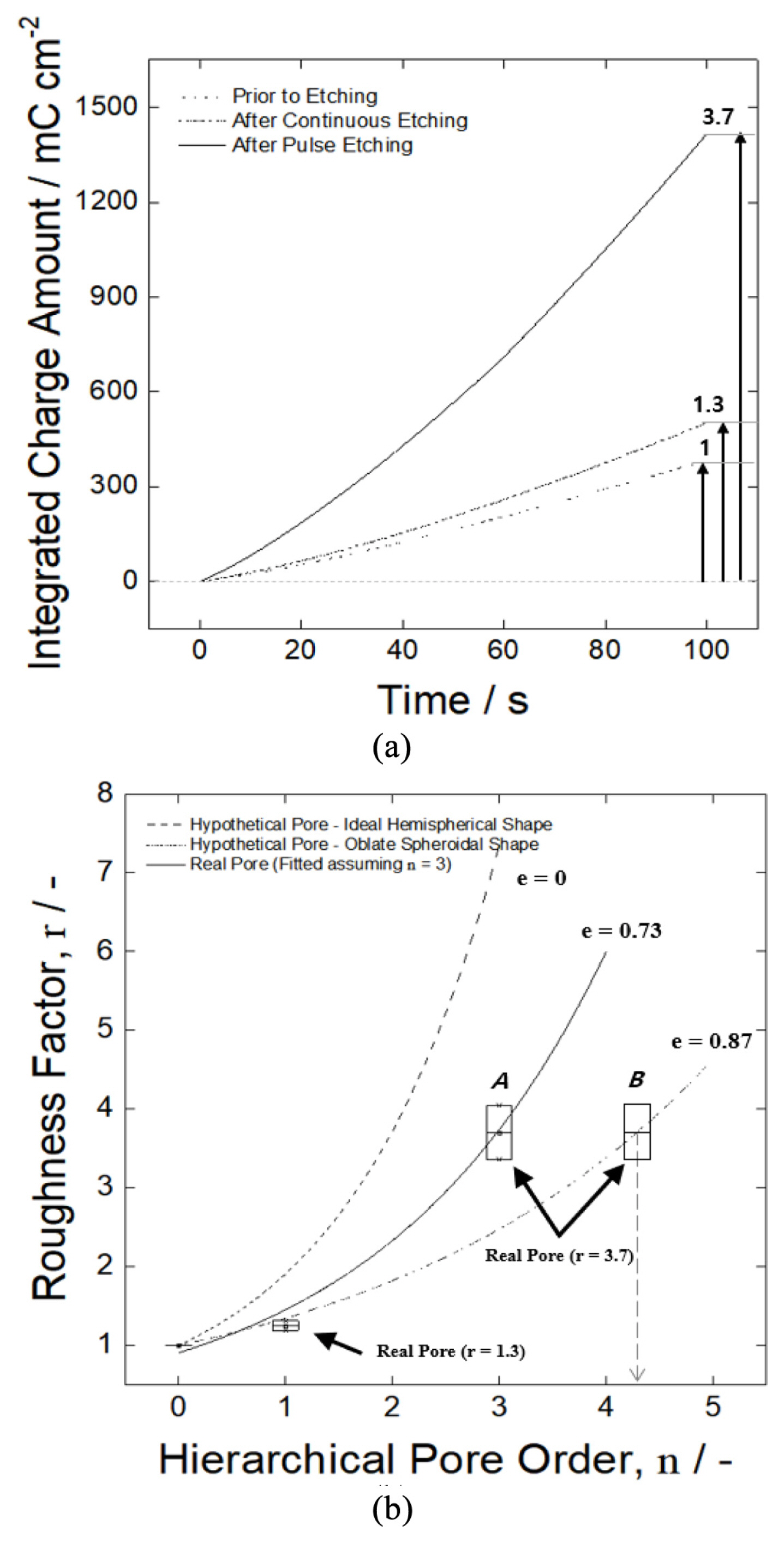
Fig. 5a shows the comparison between the rate of H
+ reduction on the flat Nb surface prior to etching and the rates on the porous surfaces obtained from the continuous (
Fig. 1c, d) and pulse etching (
Fig. 3) processes. The rate of H
+ reduction over the Nb surface containing only primary pores, formed through the continuous etching process, was approximately 1.3 times higher than that over the pristine flat Nb surface. The hierarchical porous structure, produced via the pulse etching, caused a further increase in the rate of H
+ reduction, which was found to be approximately 3.7 times higher than that over pristine Nb. These findings indicate that the continuous and pulse etching processes reported herein led to a 1.3- and 3.7-fold increase in the Nb surface area (i.e., roughness factor,
r = 1.3 and 3.7), respectively.
The equation for evaluating the total surface area of a porous material, i.e.,
Eq. (7), was used to analyze the surface area of the experimentally produced porous Nb (
Fig. 5b). Firstly, the changes in the surface area were calculated as a function of the hierarchical order of the pores for two different, hypothetical porous surfaces. One hypothetical surface consisted of pores with an ideal hemispherical shape with an eccentricity,
e, of 0 and a
k value of 2. The other was based on the experimentally observed pore shapes, i.e., oblate spheroids with the major axis length (pore diameter) that is twice as great as the minor axis length (pore depth). The corresponding eccentricity,
e, and
k value was chosen to be 0.87 and 1.38, respectively. The dependence of the surface area on the hierarchical pore order of these two hypothetic cases was presented in dashed lines in
Fig. 5b.
Then, an analysis was made on the experimentally produced porous Nb. As a matter of fact, it is virtually impossible to accurately determine the hierarchical pore order of the porous structure obtained via pulse etching due to the ambiguity of the multi-layer pore shape and the limitations of the measuring devices. Nevertheless, based on the surface and side images of the porous structure obtained through an electron microscope, it is observed that at least tertiary pores were formed, although higher-order pore structures may also have been formed (
Fig. 3). Thus, while analyzing the surface area of the experimentally obtained porous structure using
Eq. (7), we considered the following two cases: (a) the pore order
n was assumed to be 3. Then, the eccentricity
e was determined to be approximately 0.73 using the experimental surface area and
Eq. (7), i.e., the pores had an oblate spheroid structure, wherein the diameter was approximately 1.45-fold greater than the depth (
A in
Fig. 5(b)). (b) It was assumed that the
e value of 0.87, determined for the primary pores, is also applicable to the higher-order pores. The hierarchical order of the porous Nb structure was accordingly calculated to be 4ŌĆō5 (
B in
Fig. 5(b)). In spite of the above discussion on pore shape and hierarchical pore order of experimentally produced porous Nb using theoretical formula, however, various deviations from the ideal porous structure (e.g. variations of pore shape, size, and aspect ratio) could exist, and the theoretical formulas derived herein include several assumptions. Thus, the proposed theoretical approach should only be used for a general understanding of the pore structures.