


1. Introduction
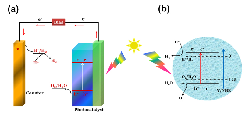
The production of energy from water using sunlight is a promising solution to reduce the demand for energy and the associated environmental concerns. In recent times, inorganic materials, such as pristine and doped TiO2 [1,2], ZnO [3,4], Fe2O3 [5],Co3O4 [6] and CdS [7] etc. have been shown to exhibit remarkable electronic and physicochemical properties and have been determined to have applications in the areas of photoluminescence [7], photovoltaics [8] and photocatalysts [9]. In general, photocatalytic semiconductors are metal oxides [10,11] or nitrides [12]. These materials act as good photo-sensitizers in photocatalytic reactions due to their filled valence band (VB) and empty conduction band (CB) in the ground state. A photocatalytic reaction occurs when these semiconductors are excited by an energy greater than the band gap, leading to the formation of excitons (i.e., electrons at the CB and holes at the VB, respectively). The direct photoelectrochemical decomposition of water can occur efficiently and sustainably, and few phenomena are essential to construct an ideal semiconductor system that must generate a sufficient voltage for irradiation to split with water, the bulk band gap must also be small enough to absorb a significant portion of the solar spectrum, and the band edge potentials at the surfaces must straddle the hydrogen and the oxygen redox potentials. Thus, the system must exhibit a long-term stability against corrosion in aqueous electrolytes, and finally, the charge transfer from the surface of the semiconductor to the solution must be facile in order to minimize the energy losses due to the kinetic over potential and must be selective for a hydrogen evolution reaction (HER) and oxygen evolution reaction (OER). The half-cell photoelectrochemical(PEC) reaction mechanism is described as follows


To date, no cost-effective materials system satisfies all technical requirements that are listed above for practical hydrogen production. Although research and development has been ongoing in order to discover materials with bulk and interfacial characteristics that meet these criteria, advances are still needed in material science and in interfacial electrochemistry. Solar to hydrogen (STH) production will play an important role in prospective sustainable-energy research because it is storable, transportable and can be converted into electricity using fuel cells whenever necessary. In addition, hydrogen is valid as feedstock in the modern chemical industry and can be used to recycle carbon dioxide via chemical processes, such as methanol synthesis and a FischerTropsch reaction.
In the present review, we focus on recent developments in novel and cost-effective photocatalytic materials to improve water splitting. The photocatalytic materials are surveyed on the basis of their photocatalytic water splitting performance. The major factors that affect the photocatalytic performance and the strategies of photocatalyst design are discussed through an overall perspective. Fig. 1a illustrates the fundamental processes in a photoelectrochemical device, for the example of a two-electrode system containing a single absorber photoanode.
2. Mechanism of Photocatalytic Water splitting
Solar PEC hydrogen production is a promising technology that could potentially provide clean, cost-effective and safe operation. Basically, when a PEC semiconductor device with the exact set of properties is immersed in an aqueous electrolyte and irradiated with external sunlight, the photon energy is converted into electrochemical energy [13] that can directly split water into hydrogen and oxygen (chemical energy). Thus the intermittent solar energy is then converted into an inherently more storable form of energy within chemical bonds. The photocatalytic water splitting reaction is an uphill reaction (Fig. 1b), and the Gibbs free energy increases by 237 kJ mol-1. The energy that is required to initiate photocatalytic and PEC water splitting is provided by light or ideally by sunlight, and in general, the water splitting mechanism of the semiconducting materials includes (i) the absorption of photon swift energies exceeding the semiconductor bandgap, leading to the generation of electron-hole pairs in the semiconducting nanoparticles, (ii) charge separation followed by migration of these photo generated carriers in semiconductor particles; (iii) surface chemical reactions between these carriers with various compounds (e.g., H2O).
Electrons and holes may also recombine with each other without participating in any chemical reactions, and semiconducting materials with smaller bandgaps or lower flat-band potentials need an external bias voltage or redox reagents to drive their action [9]. In order to facilitate the charge separation and the surface reaction, the photocatalysts and photo electrodes are modified with the corresponding co-catalysts and buffer layers. On the other hand, two or more small band-gap semiconductors can be joined to initiate the water splitting processes separately through multi photon processes. The flat band potentials are recognized to depend intensely on the ion absorption, the exposed surface area of the crystallographic orientation, surface oxidation processes and surface defects, but these factors are rarely considered during the preparation and testing of photochemical water splitting catalysts [14]. All of these processes affect the ultimate generation of oxygen or hydrogen from the semiconductor photocatalyst system. Moreover, the efficient charge separation and fast charge carrier transport that avoid any bulk/ surface charge recombination are essential for photocatalytic water splitting. The aqueous solutions containing the sacrificial reagents can be used to minimize the backward reaction (Surface back reaction effect) of H2 and O2 to water on the surface of the photocatalyst [15, 16]. Therefore, the charge separation in the photocatalyst particles and the redox reactions on their surface must proceed within the lifetimes of photoexcited carriers to successfully undertake water splitting. It is therefore important to have economical, highly efficient photocatalytic systems for light-to-energy conversion.
3. Valuation of the Efficiency
In order to engage in the photoelectrochemical decomposition of water that takes place in the PEC cells, hydrogen and oxygen are separately generated on the surface of the photo cathode and the photoanode. Normally, the photoconversion efficiency of the sample is calculated using the following equation:

where V is the applied bias vs. Reversible hydrogen electrode(RHE), I is the photocurrent density at the measured bias, and Jlight is the irradiance intensity in mW/cm2.
When compared to the photocurrent density, the photocurrent as a function of the wavelength and the IPCE is a more suitable factor to characterize the photoconversion efficiency of the different photo anodes as independent of the given light sources. IPCE can be calculated using the following equation,

where J(╬╗) is the photocurrent density (mA/cm2) that is measured, and E╬╗(╬╗) is the incident light power density (mW/cm2) for each wavelength (╬╗ in nm).
4. Nano-structured Semiconductor Photocatalyst
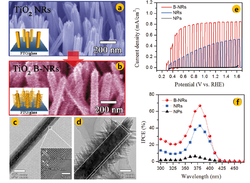
In recent years, a wide range of nano-structured semiconducting materials has been developed for use as photocatalysts under ultraviolet(UV) and visible light irradiation, PEC water splitting has progresses as a result of the unique nanostructured derived properties and effectiveness. However, some semiconductors have large band gaps (>3 eV) that limit the absorption of visible light, and thus the improvement of solar energy conversion efficiency [16]. Numerous methods, such as doping heteroatoms and using photosensitive dyes or quantum dots (QDs) have been adopted to harvest visible light [17,18]. It is well known that Titanium dioxide (TiO2) has always been considered to be an efficient photocatalyst to cleave water into hydrogen and oxygen due to the abundance, chemical stability, low cost, relatively low toxicity, superior photo stability, and high intrinsic catalytic activity under UV illumination. However, TiO2 has a large optical-band gap (3.2 eV for anatase and 3.0 eV for rutile), a low electron mobility, and short minority carrier (hole) diffusion length (10-100 nm). Thus, the photoelectric conversion efficiency of a pure TiO2 photoanode is very low, even in the UV region [19,20]. Furthermore, the one-dimensional (1D) TiO2 nanostructures (nanowires and nanotubes) can provide the advantage of a high surface area and a rapid diffusion in a single direction, yielding a low recombination of electron-hole pairs. Sun Cho et al. reported on the hierarchically-branched TiO2 nanorod structure that is shown in Fig. 2, and this branched TiO2 serves as the model architecture to have efficient photoelectrochemical devices since it instantaneously offers a large contact area with the electrolyte, excellent light-trapping characteristics, and a highly conductive pathway for charge carrier collection [21]. Paulose et al. [22] prepared 45 ┬Ąm (length) sized TiO2 nanotubes with an anodizing technique, and they achieved a photocurrent of 26 mA cm2 with a conversion efficiency of 16.25 % under UV irradiation for 45 ┬Ąm (length) sized TiO2 nanotubes calcined at 550 Ōäā. The photoelectrochemical cell based on mesoporous TiO2 films was prepared by Hartmann et al. [23] via the sol-gel method, and these Mesoporous TiO2 thin films were approximately ten times more efficient than their crystalline TiO2 nanoparticles due to their thick, continuous pore walls and lower recombination rate. However, the stability and efficiency are often compromised of these strategies, limiting the practical large-scale applications. Therefore, a large quantity of dopant species has been recently introduced by the scientific community in order to improve their applicability in practice. The role of the dopants on the TiO2 material properties remains challenging, and a quantitative understanding of the dopant combination, and whether dopants are active or inactive, and the changes in crystallinity and composition that accompany the thermal treatment that is used for activation are among the issues that must be understood in order to improve the efficiency of the photoanodes for water splitting. A modification of the TiO2 properties has succeeded mainly through (i) doping with altered transition metal ions [24] (such as Cr [25], Co [26], W [27], Zr [28]and Fe [29]), and with diverse anions such as N [30], F [31], S [32], B [33], C [34,35] to replace oxygen in the crystal lattice, and (ii) by surface decoration, which includes coupling with other semiconductors and the deposition of particles of noble metals due to the various advantages, including a higher carrier mobility, greater chemical and thermal stability, and low toxicity, which makes them efficient for use as photocatalysts.
Fig.┬Ā2.
Field effect-scanning electron microscopy(FE-SEM) images of TiO2 nanorods (NR) and branched nanorods, (c-d) high resolution TEM images of TiO2 nanorods (NR) and branched TiO2 NRŌĆÖs. (e) Linear sweep voltammetry measurements under dark and simulated sunlight illumination with a scan rate of 20 mV s-1 for TiO2 Branched Nano rods, Nano rods and Nano particles. (f) The IPCE spectra measured at 1.23 vs. RHE for the four photoanodes. Reprinted with permission [21].
Our strategy consists of identifying the semiconducting metal oxides with band-gaps that are smaller than titanium with processing that is compatible with TiO2. Therefore, we have focused our attention on Iron oxide. Regarding other semiconductors, Scot Warren et al. [36] recently reported that, hematite has many potential advantages for hydrogen or for oxygen production in PEC cells. This is an n-type semiconductor that is stable in most electrolytes at pH > 3 and has a relatively narrow bandgap, 2-2.2 eV, which is sufficient to utilize ~ 40 % of incident sunlight. Furthermore, it is an abundant, inexpensive, and environmentally benign, and it is stable in an aqueous environment under typical operating conditions. Recently, the performance of PEC based on hematite has been observed to be hindered by the short-hole diffusion length that places a constraint on the active layer thickness and its light absorption capability, as shown in Fig. 3i. In this work, Yongcai Qiu et al. [37] designed and fabricated a novel PEC device structure with ultrathin hematite films deposited on three-dimensional(3D) nanophotonic structures. Using this approach, the nanophotonic structures can largely improve the light absorption in the ultrathin active materials. Despite having these advantages, hematite exhibits a low electrical mobility, a short hole diffusion length (2 to 4 nm), and it thermodynamically requires an applied over potential to overcome an energy band misalignment [38]. Most work has thus been devoted to doping iron oxide with heteroatoms as a means to improve performance [39,40]. In addition the energy of the conduction band edge relative to the redox level of H+/H2 is thought to hinder the charge transfer for the reduction reaction [39,41-43].
Fig.┬Ā3(i).
(a) The 3D Nanospike Photonic (NSP) array photoelectrode structure, (b-c) SEM image and Cross-sectional SEM images of nanoimprint of squarely ordered nanoindentation of Al foil respectively. FE-SEM images of 3D NSP photoelectrode. Sixty degree tilted SEM images of 1000 nm pitch NSP with NSP height of about (d) 1100 nm and (e) Sixty degree tilted SEM view of Fe2O3 decorated NSPs, (f) Linear sweep voltammetry (LSV) curves of the undoped hematite photoelectrode and the Ti-doped hematite photoelectrode obtained in 1 M NaOH solution (pH 13.6) and at 20 mV s-1 scan rate. Reprinted with permission [37]. (ii). (a-d) SEM images of prepared diffent sized Au nanodot arrays, (e) PEC experimental setup schematic diagram and (f) Current vs voltage profile with light and dark condition from 0.3 to 1.1 V (vs SHE) at a scan rate of 5 mV s-1 for water splitting. . Reprinted with permission [44].
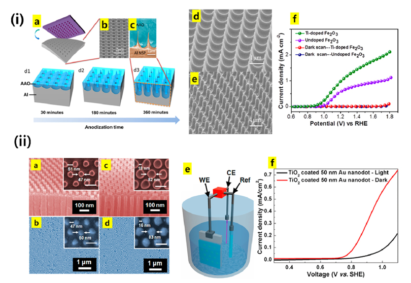
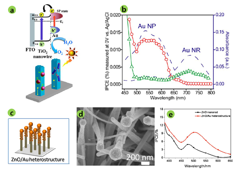
In addition, the plasmonic nanostructures have been observed to attract a considerable amount of attention in energy-harvesting areas due to their strong interaction with light through the excitation of the surface plasmon resonance (SPR) [44,45]. The frequency and the intensity of SPR are strongly related to the size, composition, shape, and nature of the nanostructures, making it possible to design plasmonic structures that interact with the entire solar spectrum and beyond. Chandrasekaran et al. [46] have lately described that the monolayer and the multilayered PEC water splitting of gold artichokes exhibit a photocurrent density of ~0.53 mA/cm2 at 1.23 V vs. RHE with an incident photon to current conversion efficiency of 1.32% under UV light irradiation. Hyung Ju Kim et al. [44] indicated that the photoelectrochemical water splitting reaction increased as the Au (gold) nanodot size decreased. Due to these precisely-controlled Au nanodot arrays, the effects of the Au nanodot size and the TiO2 overcoats were investigated for the photoelectrochemical water splitting (Fig. 3ii). The plasmon-enhanced solar-to-energy conversion efficiency in these systems has also been ascribed to three possible mechanisms. (i) The SPR induces light absorption and the subsequent transfer of hot electrons from plasmonic nanostructures to the conduction band of the semiconductors that are in contact, (ii) the near-field electromagnetic enhancement can amplify the absorption of light and can increase the generation and separation rates of the electron-hole pairs in the semiconductor, (iii) the scattering of the resonant photons can increase the length of the average photon path in the composite photoactive materials. Fig. 4 shows the interesting photoactive properties of the plasmonic nanostructures that have been assembled with wide band gap semiconductors, such as TiO2 [24,47], Fe2O3 [48], and ZnO [49] in order to fabricate materials for visible-light-responsive PEC electrodes. Chih Kai Chen et al. reported on near-infrared-driven photoelectrochemical water splitting using a ZnO nanorod-array decorated with CdTe quantum dots and plasmon-enhanced upconversion nanoparticles (Au). The plasmon enhanced the intensity of the upconversion emission, and this improved the photocurrent and the hydrogen and oxygen gas evolution rate in the PEC cell. Even though these nanostructures enhance the efficiency of the PEC [50,51], further improvements in the cost effectiveness of the device performance are required to make them commercially viable.
Fig.┬Ā4.
(a-b) PEC water spltting mechanism of Au NP/TiO2 and IPCE response values of Au nanorods and nano particles based electrodes. Reprinted with permission [47]. (c) Schematic diagram and FE-SEM image of ZnO/Au heterostructure, (e) PEC Water splitting performance of Pristine ZnO and ZnO/Au hetrostructure. Reprinted with permission [51].
5. Tailoring property of graphene in Nanostructured Inorganic Photocatalyst
Graphene is an ideal material to mediate the photogenerated charge for water splitting. Graphene-based materials have been extensively investigated as a result of their superior physical and chemical properties resulting from their unique two-dimensional (2D) honey-comb layer structure with sp2 hybridized carbon atoms for their electronic and optoelectronic properties [52]. The studies to improve their processibility have also been extensively reported, and the low density of Graphene and reduced graphene oxide(RGO) makes them exceptionally good candidates for use in numerous applications, such as in the aerospace industry where highly-specific mechanical and physical properties are needed. These materials have been extensively considered to be catalyst supports due to their unique properties, such as large specific surface area, excellent mechanical and electrical properties [53].
6. Tuning the electronic properties of graphene
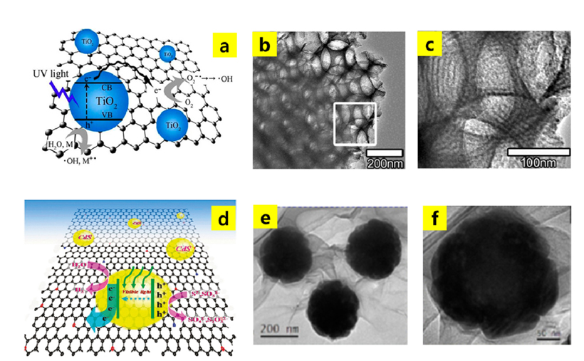
Heteroatoms or functionalities have been introduced to extend the applicability of graphene to the photocatalysis processes. For example, the electronic properties of graphene can be readily tuned by covering them with oxygen atoms, and the oxygen adsorption removes the equivalence of the two carbon sublattices in graphene by forming C-O covalent bonds that damage the original orbitals. This coverage results in the split-up of damaged ŽĆ and ŽĆ * orbitals and creates a band gap in the graphene. More oxygen can be introduced to extend the band gap, and the valence band maximum (VBM) gradually changes from the ŽĆ orbital of graphene to the 2p orbital of oxygen while the ŽĆ * orbital remains as the conduction band minimum (CBM). graphene oxide(GO) is the intermediate state between graphene and graphite, and it can be synthesized using HummersŌĆÖ method [53], which uses chemical oxidation to exfoliate graphite and is readily scalable. The RGO, chemically modified GO, and GO-based nanocomposites can be obtained using various techniques, including hydrothermal, solvothermal, etc.[54]. Both GO and RGO contain the oxygen functional groups on their graphene sheets, but with different oxygenation levels. The addition of semiconducting materials with nanostructured carbon materials (such as fullerenes, carbon nanotubes, and GO sheets) has unique advantages in suppressing the charge recombination. The GO sheets are particularly effective to separate the charges on TiO2 on account of their 2D profiles [55,56]. Also, the unpaired ├░ electrons on GO can bond with the surface Ti atoms of TiO2 to form Ti-O-C bonding and can extend the light absorption range of TiO2, as shown in Fig. 5a-c [57,58]. In general, the GO-TiO2 composites exhibit an outstanding photochemical response under light irradiation. W. Fan et al. reported on GO-TiO2 hybrid materials that were used to harness the photon energy to generate H2 from water decomposition [59]. The GO-TiO2 nanocomposites that were synthesized using a sol-gel method with subsequent calcination exhibited a PEC activity that was 1.9 times that of pure TiO2 in an aqueous polysulfide solution under illumination with an Xe-lamp [60]. These results suggest that GO is an electron transport mediator that can facilitate charge separation. RGO was reported to be able to trap electrons from UV irradiated TiO2 via the percolation mechanism and to transport the trapped electrons in order to reduce the silver ions into silver nanoparticles. These conclusions prove directly that the photo-induced electrons could transfer from TiO2 to RGO in order to avoid their combination with holes [53]. Thus, graphene is an electron acceptor and a transporter that can promote the separation of the photo-generated electron-hole pairs in the semiconducting TiO2, efficiently transport photogenerated electrons to reactive sites, and finally improve the PEC water splitting performance. As an electron acceptor and transporter, graphene has been extensively investigated in order to achieve controllable PEC activities in graphene-TiO2 nanocomposites by varying the graphene content [61]. Chandrasekaran et al. [62] prepared RGO-Fe2O3 photocatalysts for PEC water splitting, and they found that the sample calcined at 500 Ōäā exhibits a higher PEC performance. These results indicate that the photocatalytic performance of iron oxide can be significantly improved via hybridization with GO and the calcination process, the RGO serves as an electron sink to facilitate the exciton separation and to store the separated electron. There, an IPCE of the 500Ōäā-calcined RGO-Fe2O3 was found to be ~4 times higher than that of pure iron oxide. Even though, the various visible-light-driven photocatalysts have been reported, CdS is an attractive material for PEC water splitting because it has a narrow bandgap of 2.4 eV that can absorb an appreciable portion of visible light. The photocatalytic activity of the CdS semiconductor is limited by the high recombination rate of the photo induced electron-hole pairs. But, after the addition of graphene, the photocatalytic activity has improved for the CdS nanoparticles (Fig. 5d-f) [63-65]. Li et al. investigated the photocatalytic properties of the RGO-CdS nanocomposites that were prepared using a solvothermal method where the reduction of the GO and the deposition of CdS on RGO were simultaneously achieved [66]. This photocatalaytic performance was a result of the large surface area of the GO that offers greater active adsorption sites in a photocatalytic reaction center. Cao et al. specified an ultrafast picosecond electron transfer process from the photoexcited CdS to the graphene sheets in the graphene-CdS nanocomposites using time-resolved florescence spectroscopy [67]. This work validated the fact that graphene could act as an electron acceptor and as a transporter to reduce the recombination rate of the photo-induced electron-hole pairs in the CdS photocatalysts. Lately, Mou et al. [68] prepared a novel TiSi2-RGO composite that uses RuO2 as a cocatalyst for water splitting under visible light irradiation. The resulting RuO2-TiSi2 -RGO composite showed a higher rate of PEC performance than both the RuO2-TiSi2 composite and pristine TiSi2. Herein, they have specified that RGO sheets serve as electron acceptors, trapping the photogenerated electrons from TiSi2 and/or RuO2 particles and reducing the probability of electron-hole recombination. O2 simultaneously evolved at high temperatures through the oxidation of water by holes in the VB of TiSi2.
Fig.┬Ā5.
(a) Schematic Illustration of Incorporating TiO2 with RGO to the Formation of RGO/TiO2 Nanocomposites and Proposed Mechanism of the RGO/TiO2 Composites. Reprinted with permission [57]. (b and c) TEM micrographs of macro- mesoporous titania films with graphene. Reprinted with permission [58]. (d) The formation GO-CdS composites, where GO sheets as an electron sink to facilitate exciton separation and store the separated electrons. Reprinted with permission [64]. (e-f) FE-SEM images of homogeneous deposition of CdS nanoparticles on a GO sheet. Reprinted with permission [65].
Actually, graphene itself can also be used as a dopant for wide bandgap photocatalysts to be active in the visible light region, which is analogous to the case of a carbon-doped semiconductor. Ng et al. [69] first demonstrated that graphene can improve the O2 and H2 production rate in the PEC cells. As is shown in Fig. 6, the working photo electrode was fabricated using a spin-coating technique with BiVO4-RGO composites. There, the IPCE showed an increase of 4.2 % for the BiVO4-RGO in contrast to that of BiVO4. The improvement was assigned to the usefulness of RGO in promoting the charge collection and transport by accepting the photo-generated electrons from BiVO4 and shuttling them to the collecting electrode, as well as improving the contact between the BiVO4 particles and the transparent conducting electrode after using the RGO as a scaffold. These observations, indicate that coupling the two photocatalyst can effectively improve the photocatalytic efficiency, as shown in Fig. 7 [65,70,71]. Moreover, the decoration of GO with semiconducting materials makes more photo-induced holes contribute to the oxidation current under illumination. Even though the nano-sized materials exhibit a good PEC water splitting performance, the photocatalytic activity of the RGO-Metal oxide nanocomposite was higher than that of the pure metal oxide due to the improvement in light absorption and the acceleration in the charge separation when metal oxide is anchored on GO. The overall photocatalytic water splitting performance of various types of photocatalytic materials is presented in Table 1.
Fig.┬Ā6.
(a) PEC water splitting mechanism of RGO-BiVO4 nanocomposites, (b) LSV curves and (c) IPCE values of pure TiO2, BiVO4 and RGO-BiVO4 composites. Reprinted with permission [43].
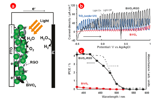
Fig.┬Ā7.
(a) Schematic diagram for the Energy Band Structure of Fe2O3 NR-RGO-BiV1xMoxO4 Heterojunction and Proposed Mechanism of PEC Water Splitting, (b-d) TEM images of the Fe2O3 NR-RGO-BiV1xMoxO4 Heterojunction, (e and f) LSV curves of prepared pristine, composites and their corresponding efficiency values respectively. Reprinted with permission [71].


7. Conclusion
This paper reviews the progress to date of the research on photocatalytic water splitting in terms of both the outcomes and challenges in this field. Since the quantum efficiency that is acquired over the present photocatalysts is not yet satisfactory to ensure practical applicability, a more efficient visible-light-driven photocatalysts should be developed, and it is necessary to narrow the band gap of the photocatalysts to harvest visible-light in the longer wavelength region and to improve the photo-generated charge separation in photocatalysis. The factors electronic properties, chemical composition, structure and crystallinity, surface states and morphology determine the photocatalytic activity of the materials to further reveal them in sufficient detail. Lower cost, alternative co-catalysts, such as non-noble metals and derived metal compounds, should be tested for their suitability as substitutes for the most frequently used noble metals, which is very inventive but expensive. Photocatalyst-free noble metals are also highly preferred considering that such photocatalysts can be readily used in a more economical way. From this point of view, graphene-incorporated nanostructures have been further developed. The intense efforts and close cooperation among researchers in different fields result in great breakthroughs for hydrogen energy development by utilizing graphene-based materials, which we believe will be far beyond what has been reported in this review paper and will be beneficial for human beings in terms of both the economic and environmental aspects.


