Enhanced Efficiency of Nanoporous-layer-covered TiO2 NanotubeArrays for Front Illuminated Dye-sensitized Solar Cells
Article information
Abstract
Nanoporous-layer-covered TiO2 nanotube arrays (Type II TNTs) were fabricated by two-step electrochemical anodization. For comparison, conventional TiO2 nanotube arrays (Type I TNTs) were also prepared by one-step electrochemical anodization. Types I and II TNTs were detached by selective etching and then transferred successfully to a transparent F-doped SnO2 (FTO) substrate by a sol-gel process. Both FTO/Types I and II TNTs allowed front side illumination to exhibit incident photon-to-current efficiencies (IPCEs) in the long wavelength region of 300 to 750 nm without the absorption of light by the iodine-containing electrolyte. The Type II TNT exhibited longer electron lifetime and faster charge transfer than the Type I TNT because of its relatively fewer defect states. These beneficial effects lead to a high overall energy conversion efficiency (5.32 %) of the resulting dye-sensitized solar cell.
1. Introduction
Mesoporous TiO2-based dye-sensitized solar cells (DSSCs) are potential low-cost alternatives to commercial Si solar cells [1-4]. These cells comprise a dye-sensitized TiO2 photoanode and a Pt counter electrode with an electrolyte incorporating a redox couple (I/I3) between them.
To improve the cell performance, the surface morphology and/or particle size of TiO2 layers has been controlled [5,6], and new dyes [7] and electrolytes have been developed [8]. Conventional TiO2 films consisting of nanoparticles smaller than 30 nm do not establish a depletion layer at the TiO2/electrolyte interface. This causes significant back electron transfer from the conduction band of the TiO2 to the electrolyte due to defect trap-limited diffusion. Back electron transfer has been hindered using 1-dimensional (1-D) nanostructures (nanotubes, nanorods, etc.) with rapid electron transport and slow recombination rates [4-6,9,10].
TiO2 nanotube arrays (TNTs) have been fabricated by electrochemically anodizing Ti metallic foils in an F- ion-containing solution. The TNTs grown on the Ti metallic foils only allow back side illumination because of the opaqueness of the Ti metal. With back side illumination, the counter electrodes (CEs) should be as transparent as possible, otherwise they will reflect light and the iodine-based electrolytes will absorb photons, which reduces the level of light harvesting significantly [10,11]. Recently, to overcome this problem, front side-illuminated TNTs have been recognized by transferring free-standing TNTs to transparent fluorine-doped tin oxides (FTOs) substrates [11-13].
In this article, two types of TiO2 nanotubes arrays (TNTs) were synthesized: the conventional TNT (Type I TNT) fabricated by one-step electrochemical anodization and the nanoporous-layer-covered TNT (Type II TNT) fabricated by two-step electrochemical anodization. Both TNTs were then transferred to the transparent FTO for front side illumination, which allowed light harvesting of the dye molecules without the loss of photons by light reflection and absorption. In particular, the Type II TNTs had relatively fewer defect states compared to the Type I TNTs, hindering the defect-mediated recombination rate significantly. As a result, the FTO/Type II TNT exhibited much longer electron lifetime and faster charge transfer, giving rise to a significant enhancement of the overall energy conversion efficiencies. The significantly improved performance of the DSSC with the FTO/Type II TNT was studied in terms of the morphology, electron lifetime, charge transfer, recombination rate, and incident photon-to-current efficiency (IPCE).
2. Experiment
2.1. Conventional TiO2 nanotube array (Type I TNT)
Ti foil (Good fellow) was used for the anodic growth of TiO2 nanotube arrays. The foil was ground roughly, cleaned by sonication in acetone and ethanol, and then rinsed in de-ionized (DI) water. Electrochemical anodization was conducted at 60 V for 3 h with an approximate 4 cm separation between the working electrode of the Ti foil and the counter electrode (Pt mesh). The electrolyte consisted of 0.25 wt.% NH4F in ethylene glycol containing a trace amount of water. The 15.5 µm-thick anodic TiO2 nanotubes were sonicated in ethanol for 5 min to remove the remnants from the surface and then dried in an air. They were then annealed at 450 ℃for 30 min in air for the formation of crystalline TNTs.
2.2. Nanoporous-layer-covered TiO2 nanotube array (Type II TNT)
The pretreated Ti substrates were first prepared by the 1-step electrochemical formation of conventional TiO2 nanotubes. They were then removed from the Ti substrate by sonication in DI water for 5 min. A second anodization step was performed under similar conditions to those of the 1-step TiO2 nanotubes to form the 15.5 µm-thick, nanoporous-layer-covered TiO2 nanotube arrays [4,14]. The resulting 2-step TiO2 nanotubes were sonicated in ethanol for 5 min to remove the remnants, followed by drying in air. They were then annealed at 450 ℃ for 30 min in air to convert the amorphous structure to an anatase crystalline TNT (Type II TNT).
2.3. Transferring procedure of the TNTs onto the transparent FTO substrates
The Ti foil/crystalline TNTs (Types I and II) were anodized again in the same stock electrolyte for 3 h with a potential of 20 V to form an amorphous TiO2 layer between the crystalline TNT (c-TNT) and Ti foil [15]. The samples were then immersed into a 5% H2O2 solution for 2 h to etch the amorphous TiO2 selectively, leading to free-standing c-TNTs. The freestanding c-TNTs were then adhered to the FTO substrates with one drop of the Ti precursor-containing sol (0.1 M titanium isopropoxide (TTIP) in isopropanol and 5 wt.% ethyl cellulose). The resulting films were then annealed at 450 ℃ for 30 min in air for the interconnection between the FTO and TNTs by the formation of a thin TiO2 interlayer.
2.4. Cell Fabrication
The FTO/Types I and II TNTs were dye-sensitized with the Ru-based N3 dye [cis-bis (4,4’- dicarboxy-2,2’-bipyridine) dithiocyanato ruthenium (II)] (Solaronix SA, Switzerland) by immersion in the dye solution at 40 ℃ for 24 h. Semitransparent Pt counter electrodes were prepared by doctor-blading a Pt nanocluster-containing Pt paste (PT-1, Dyesol Ltd.) onto the FTO transparent conducting substrates followed by calcination at 450 ℃ for 30 min in air. The dye-adsorbed TNT photoanodes and Pt counter electrodes were sandwiched with a liquid electrolyte containing the redox couple (I/I3) introduced between them.
2.5. Characterization
The DSSCs with the FTO/TNTs were illuminated from the front side through the FTO/TNTs. Their photovoltaic current-voltage characteristics were measured using a solar simulator (PEC-L11, PEC cell Ltd.) under 1 Sun illumination (100 mWcm2 , AM 1.5), which was verified using an AIST-calibrated Si-solar cell. The Nyquist plots were measured between 1 Hz and 100 kHz using an electrochemical impedance analyzer under 1 Sun at the open-circuit potential.
For the open-circuit voltage decay (OCVD) measurements, the cells were illuminated to a steady voltage. The illumination was then cut off using a shutter. The decay analyses refer only to the values measured after the shutter obtained full darkness. The incident photon-to-current conversion efficiency (IPCE) was measured using an action spectrum measurement setup (PEC-S20, PEC cell Ltd.) in DC mode without the white bias. The morphologies of the FTO/TNTs were characterized by field-emission scanning electron microscopy (SEM, Hitachi FE-SEM S4800). All samples had similar active areas of dye-adsorbed photoanodes, 0.24 cm2 .
3. Results and Discussion
Fig. 1 presents FE-SEM surface images viewed (a, c) from the top of the FTO/Type I TNT and (b, d) from the top of the FTO/Type II TNT. The insets of Figs. 1c, 1d clearly show the Types I and II TNTs transferred successfully onto the FTO substrates by the formation of the TiO2 interlayer, in which both of Types I and II TNTs exhibited similar thicknesses of 15.5 µm. The thickness of the TiO2 interlayer was approximately 750 nm for both. The Type I TNT was composed of separated nanotubes with a mean diameter and wall thickness of 96 and 24 nm, respectively, as shown in Fig. 1(c). Fig. 1(d) and its inset showed that each nanopore corresponds to one nanotube with a mean diameter and wall thickness of 92 nm and 21 nm, respectively, and the void areas of the surface are covered by a thin nanoporous TiO2 layer [14]. The conventional TNT (Type I sample) exhibited bundling of the nanotubes, as shown in Fig. 1(a) by the liquid-meniscus-induced capillary forces, which causes many microcracks that act as defect staterelated recombination centers [14]. In contrast, the Type II TNT has relatively fewer defects. This is because the surface-interconnected nano-pores by the thin nanoporous TiO2 help keep the nanotubes in a parallel arrangement and prevent them from being bundled, as shown in the Fig. 1b.

FE-SEM surface images viewed (a, c) from the top of the FTO/Type I TNT and (b, d) from the top of the FTO/ Type II TNT. The insets in the (c) and (d) show crosssectional SEM images of the FTO/Types I and II TNTs, respectively.
The electron lifetimes were estimated through open-circuit voltage decay (OCVD) measurements [16]. Fig. 2a shows the Voc decay curves of the DSSCs with the Types I and II TNTs recorded during relaxation from an illuminated quasi-equilibrium state to the dark equilibrium. Fig. 2b presents the electron lifetimes calculated from the OCVD curves of Fig. 2a, according to the following equation [16]:

(a) Voc decay curves of the DSSCs with the Types I and II TNTs recorded during relaxation from an illuminated quasiequilibrium state to the dark. (b) Electron lifetimes calculated from (a).

where kBT is the thermal energy, e is the positive elementary charge and dVoc/dt is the derivative of the open circuit voltage transient. The photo voltage decay rate is related directly to the electron lifetime. This is because, as the illumination of the DSSC at open circuit is interrupted, excess electrons are removed through recombination from the TiO2 to the redox couple according to I3- + 2e- (TiO2) → 3I-. Although the TiO2 interlayer was employed between the FTO and TNTs (Types I and II), a significant difference in the electron lifetime was observed between the Types I and II TNTs, indicating that the electron lifetime was barely affected by the TiO2 interlayer. The Type II TNT exhibited a much longer electron lifetime than the Type I TNT (conventional TNT). This can be because, unlike the Type I TNT, the Type II TNTs are composed of well-aligned nanotube arrays without bundling, which decrease the number of surface defect-related recombination traps and suppresses the defectmediated recombination rate.
Electrochemical impedance spectroscopy was performed to characterize the electron transporting properties in more detail. Fig. 3 shows Nyquist plots of the DSSCs with the FTO/Types I and II TNTs measured at the open circuit voltage (Voc) under 1 Sun illumination. The Nyquist plots showed two distinct semicircles, where the semicircles at high- and low-frequencies are related to electrochemical reaction resistance at the Pt counter electrode (R2, inset Fig. 3) and charge transfer resistance at the TiO2/dye/electrolyte (R3, inset Fig. 3)[17]. The FTO/Type II TNT exhibited a much smaller R3 value, indicating faster charge transfer kinetics. From Fig. 1, the Type II TNT showed very well-aligned nanotube arrays without bundling, giving rise to much fewer defect states. The significantly reduced surface defect states of the FTO/Type II TNT can not only suppress the defect-mediated recombination rate, but also facilitate electron transport, leading to a significantly enhanced τe and fast charge transfer.

Nyquist plots of the DSSCs with the FTO/Types I and II TNTs measured at the open circuit voltage (Voc) under 1 Sun illumination. Inset shows an equivalent electrical circuit.
Fig. 4a shows the photovoltaic current-voltage curves of the DSSCs with the FTO/Types I and II TNTs measured under 1 Sun illumination, as listed in Table 1. These results were reproducible. The amounts of N3 dye adsorbed, which was measured by UV-Vis spectroscopy, were 7.56 × 10⁻⁹ and 7.34 × 10⁻⁹ molcm-2 for the FTO/Type I and FTO/Type II TNTs, respectively. Despite the similar dye contents, the DSSC with the FTO/Type II TNT provided a significantly improved overall energy conversion efficiency (5.32 %), due mainly to the enhanced short-circuit current (Jsc). To confirm the enhancement of the Jsc and study it in more detail, the incident photon-to-current efficiency (IPCE) curves were measured, as shown in Fig. 4b. The IPCE is influenced mainly by three factors, according to:[18]

(a) Photovoltaic current-voltage curves of the DSSCs with the FTO/Types I and II TNTs measured under 1 Sun illumination. (b) IPCE curves.
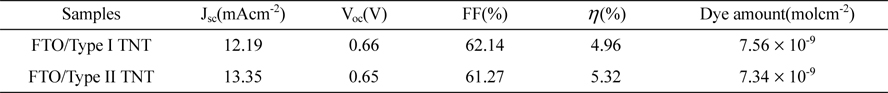
Photovoltaic performances and the amount of the attached dye molecules for the FTO/Types I and II TNT

where the LHE and ηinj are the light-harvesting efficiency and the charge-injection efficiency, respectively. ηinj is close to unity due to the rapid electron injection from the excited N3 dye to TiO2. The LHE was determined by the amount of adsorbed dye, light scattering and the concentration of redox species. The FTO/Types I and II TNTs showed a similar amount of adsorbed dyes, indicating a similar LHE value. Note that the TNTs were transferred to the FTO transparent conducting substrates by the selective etching and solgel process, which allows front-side illumination. The DSSC with the Ti foil/TNT should be illuminated on the back side, due to the opaque Ti metallic foil. The back-side illuminated DSSC has no apparent IPCE value below 450 nm due to the light absorption of the iodine-containing electrolyte and light scattering of the Pt counter electrode [4]. Fig. 4b clearly shows that the DSSCs with the FTO/Types I and II TNTs exhibit IPCE values in the long wavelength from 300 to 750 nm without any IPCE loss by the electrolyte and counter electrode due to the allowed front-side illumination. ηcc is determined by the competition between recombination and charge transport. In Figs. 2-3, the FTO/Type II TNTs provided a significantly enhanced electron lifetimes and facilitated charge transfer, contributing to an improved ηcc. Therefore, the significantly increased cell efficiency of the DSSC with the FTO/Type I TNTs can be attributed to the remarkably enhanced charge collection performance that increases the Jsc value.
4. Conclusions
A nanoporous-layer-covered Type II TNT on the FTO substrate was fabricated by two-step electrochemical anodization followed by a selective etching and sol-gel process. For comparison, the conventional Type I TNT on the FTO was also prepared. The DSSCs with the FTO/Types I and II TNTs allowed front-side illumination to prevent any IPCE loss by light absorption of the electrolyte and the light scattering of the Pt counter electrode, leading to good IPCE values, even below the wavelength of 450 nm. In particular, the FTO/Type II TNTs exhibited relatively fewer surface defects due to well-aligned nanotube arrays supported by the nanoporous TiO2 thin layer on top of the arrays. As a result, the FTO/Type II TNT provided not only longer electron lifetime, but also faster charge transfer in the TiO2 network, which contributed to the significantly enhanced charge collection efficiency and cell efficiency, as high as 5.32 %. These results provide insight into 1-D nanostructured electrodes for a range of applications, such as solar cells, catalysts and photoelectrochemical cells.
Acknowledgements
This research was supported by Basic Science Research Program through the National Research Foundation of Korea (NRF) funded by the Ministry of Education (NRF- 2015R1D1A3A01016158). This work was also supported by “Human Resources Program in Energy Technology” of the Korea Institute of Energy Technology Evaluation and Planning (KETEP), granted financial resource from the Ministry of Trade, Industry & Energy, Republic of Korea (No. 20154030200760).
References
B. O’Regan and M. Grätzel, Nature, 353, 737 (1991).
O’Regan B., Grätzel M.. Nature (1991);353:737. 10.1038/353737a0.J. Kwon and J. H. Park, J. Electrochem. Sci. Technol., 4, 89 (2013).
Kwon J., Park J. H.. J. Electrochem. Sci. Technol. (2013);4:89. 10.5229/JECST.2013.4.3.89.M. Grätzel, Nature, 414, 338 (2001).
Grätzel M.. Nature (2001);414:338. 10.1038/35104607.J.-H. Park, J.-Y. Kim, J.-H. Kim, C.-J. Choi, H. S. Kim, Y.-E. Sung and K.-S. Ahn, J. Power Sources, 196, 8904 (2011).
Park J.-H., Kim J.-Y., Kim J.-H., Choi C.-J., Kim H. S., Sung Y.-E., Ahn K.-S.. J. Power Sources (2011);196:8904. 10.1016/j.jpowsour.2011.06.063.G. K. Mor, K. Shankar, M. Paulose, O. K. Varghese and C. A. Grimes, Nano Lett., 6, 215 (2006).
Mor G. K., Shankar K., Paulose M., Varghese O. K., Grimes C. A.. Nano Lett. (2006);6:215. 10.1021/nl052099j.Y.-C. Nah, I. Paramasivam and P. Schmuki, Chem Phys Chem, 11, 2698 (2010).
Nah Y.-C., Paramasivam I., Schmuki P.. Chem Phys Chem (2010);11:2698.S. S. Park, Y. S. Won, Y. C. Choi, and J. H. Kim, Energy & Fuels, 23, 3732 (2009).
Park S. S., Won Y. S., Choi Y. C., Kim J. H.. Energy & Fuels (2009);23:3732. 10.1021/ef900207y.S.-J. Seo, H.-J. Cha, Y. S. Kang and M.-S. Kang, Electrochimica Acta, 145, 217 (2014).
Seo S.-J., Cha H.-J., Kang Y. S., Kang M.-S.. Electrochimica Acta (2014);145:217. 10.1016/j.electacta.2014.09.016.J.-Y. Kim, K.-H. Lee, J. Shin, S. H. Park, J. S. Kang, K. S. Han, M. M. Sung, N. Pinna and Y.-E. Sung, Nanotechnology, 25, 504003 (2014).
Kim J.-Y., Lee K.-H., Shin J., Park S. H., Kang J. S., Han K. S., Sung M. M., Pinna N., Sung Y.-E.. Nanotechnology (2014);25:504003. 10.1088/0957-4484/25/50/504003.S. W. Jung, J.-H. Park, W. Lee, J.-H. Kim, H. Kim, C.-J. Choi and K.-S. Ahn, J. Appl. Phys., 110, 054301 (2011).
Jung S. W., Park J.-H., Lee W., Kim J.-H., Kim H., Choi C.-J., Ahn K.-S.. J. Appl. Phys. (2011);110:054301. 10.1063/1.3630114.Q. Chen and D. Xu, J. Phys. Chem. C, 113, 6310 (2009).
Chen Q., Xu D.. J. Phys. Chem. C (2009);113:6310. 10.1021/jp900336e.J. Choi, S.-H. Park, Y. S. Kwon, J. Lim, I. Y. Song and T. Park, Chem. Commun., 48, 8748 (2012).
Choi J., Park S.-H., Kwon Y. S., Lim J., Song I. Y., Park T.. Chem. Commun. (2012);48:8748. 10.1039/c2cc33629d.J. H. Park, T.-W. Lee, and M. G. Kang, Chem. Commun., 2867 (2008).
Park J. H., Lee T.-W., Kang M. G.. Chem. Commun. (2008);2867D. Wang, B. Yu, C. Wang, F. Zhou and W. Liu, Adv. Mater., 21, 1964 (2009).
Wang D., Yu B., Wang C., Zhou F., Liu W.. Adv. Mater. (2009);21:1964. 10.1002/adma.200801996.S. W. Jung, S.-Y. Lee, M.-A. Park, J.-H. Kim, S.-H. Kang, H. Kim and C.-J. Choi, Mol. Cryst. Liq. Cryst., 598, 144 (2014).
Jung S. W., Lee S.-Y., Park M.-A., Kim J.-H., Kang S.-H., Kim H., Choi C.-J.. Mol. Cryst. Liq. Cryst. (2014);598:144. 10.1080/15421406.2014.933386.A. Zaban, M. Greenshtein and J. Bisquert, ChemPhysChem, 4, 859 (2003).
Zaban A., Greenshtein M., Bisquert J.. ChemPhysChem (2003);4:859. 10.1002/cphc.200200615.G. Zhu, Z. Cheng, T. Lv, L. Pan, Q. Zhao and Z. Sun, Nanoscale, 2, 1229 (2010).
Zhu G., Cheng Z., Lv T., Pan L., Zhao Q., Sun Z.. Nanoscale (2010);2:1229. 10.1039/c0nr00087f.B. C. O’Regan, J. R. Durrant, P. M. Sommeling and N. J. Bakker, J. Phys. Chem. C, 111, 14001 (2007).
O’Regan B. C., Durrant J. R., Sommeling P. M., Bakker N. J.. J. Phys. Chem. C (2007);111:14001.