


1. Introduction
Numerous studies have used nanostructured metal oxides as electrode materials for high-performance electrochemical devices. In particular, 1-dimensional (1D) nanostructured metal oxides are considered to be highly effective electrodes since their nanoporous nature results in a large surface area and consequently a small activation polarization. The structure also provides a 1D pathway for facile movement of the reactants and products, thus reducing the concentration polarization. Anodization is one of the easiest methods for manufacturing 1D nanostructured metal oxides. When forming 1D nanostructures using this method, properties such as the pore diameter, length, and pore-wall thickness can be easily adjusted by controlling the anodizing conditions (e.g., voltage, time, electrolyte composition, temperature, etc.) [1-16]. Since the anodic formation of a 1D tin oxide nanoporous structure was reported [1], recent studies have focused on changing the anodizing conditions to control the nanoporous structure of 1D tin oxide, and on applying the same methodology to the electrode materials used in high-performance semiconductor-type gas sensors [3,4,13] and energy storage devices [7,12].
The size, morphology, and crystal structure of nanostructured metal oxides greatly affect their chemical, optical, and electrochemical properties [6,8,12,13,15]. In particular, the crystallinity and the crystal structure are critical parameters to consider when using nanostructured metal oxides as electrode materials in electrochemical applications, as they determine the fundamental properties of metal oxides [8,12,13,15]. However, most metal oxides formed by anodization are either amorphous or have a low degree of crystallinity owing to the high voltages applied over very short time periods. Due to this problem, many researchers have crystalized metal oxides at high temperatures. For example, crystalized anodic metal oxides can be obtained directly by anodization at high temperatures [5,9], or heat treatment can be used to subsequently crystallize the metal oxides formed by anodization [2,8,11-13,15]. Both cases incur additional costs either for maintaining high temperatures or for the post-treatment. Also, the substrate is vulnerable to being oxidized together with the metal oxide at such high temperatures.
This study presents a novel experimental finding, wherein the crystallinity of 1D nanostructured tin oxide can be altered without any heat treatment. The nanoporous structure can be retained by using different substrate materials and controlling the thickness of the tin being anodized. The factors that influence crystallization are investigated and suitable conditions for crystalizing tin oxide with this methodology are proposed.
2. Experimental Section
2.1 Preparation of materials and anodization
Two different tin specimens were anodized. Firstly, a 25 mm-thick tin foil (Alfa Aesar, 99.995%), first polished with #2000A SiC paper, treated with 0.1 M HCl to completely remove the native oxide film from the surface, then thoroughly washed with distilled water. The tin foil was anodized without any additional treatment. Secondly, a silicon (<100>, p-type, LG SILTRON) substrate with titanium (5 nm), gold (100 nm), and copper (100 nm) sequentially deposited (E-beam Evaporator, UEE-105) upon its surface, which was then coated with a thin film of tin. The gold layer does not react under the anodization conditions and acts as an electrically conductive layer, whilst the titanium layer acts as a buffer to enhance the adhesion between the silicon and gold layers. Copper is deposited in the final stage owing to its strong adhesion to tin.
To coat the as-described silicon substrate with tin, the substrate was used as a working electrode with a Pt counter electrode, separated by 1 cm. An aqueous solution containing Sn(CH3SO3)2, CH3SO3H, and aldehyde-based additives (provided by Incheon Chemicals, Republic of Korea) was used. A current density of 150 mA/cm2 was applied for different durations to form tin coatings with different thicknesses. The tin coating was formed at a rate of 1 ╬╝m per 10 s. An IviumStat (Ivium Technologies, The Netherlands) was used to control the plating.
To form tin oxide, either the tin foil or the tin-coated silicon material was used as the working electrode with a Pt wire counter electrode. An aqueous solution of 0.5 M oxalic acid (Aldrich, 98%) was used as the electrolyte, and an anodic pulse voltage was applied to the working electrode, using the IviumStat. The pulse sequence consisted of applying 8 V for 0.05 s then reverting to the open circuit potential. These steps were performed repeatedly for up to 600 cycles.
2.2 Analysis of morphology and crystallinity
The surface of each oxide was observed by scanning electron microscopy (FESEM, MIRA3, TES-CAN, Czech Republic), while the in-depth structure of specific specimens was further investigated by transmission electron microscopy (FETEM, Titan G2ChemiSTEM Cs Probe, FEI Company, The Netherlands). The crystal structure and the degree of crystallinity of the tin oxides were measured by X-ray diffraction (XRD, D8, Advance, Bruker, Germany; Ultima-IV, Rigaku, Japan), and Raman spectroscopy (ARAMI, Horiba Jobin Yvon, France).
3. Results and Discussion
Figs. 1(a), (b) and (c) show the surface images of an anodized tin foil and anodized 1 ╬╝m and 300 ╬╝m-thick tin coatings on silicon substrates; also shown are their cross-sectional images (inset figures). The tin oxide nanoporous structure was found to be well developed for both the tin foil and the silicon substrate. According to a previous study [1,17,18], anodic tin oxide created from a tin foil is usually amorphous or has a low degree of crystallinity. In this regard, the transmission electron micrograph and electron diffraction pattern of the anodic tin oxide formed on the silicon substrate (Fig. 1(d)) are remarkable. The micrograph shows a lattice structure and the diffraction pattern displays clear rings that can be attributed to crystalline tin oxide, SnO2. Since tin oxide was formed quickly at a high voltage and room temperature, it is anticipated that its structure is amorphous or, at best, of very low crystallinity. Therefore, the clear observation of crystallinity when using a silicon substrate is unexpected and highly noteworthy.
Fig.┬Ā1.
Scanning electron micrographs of the surfaces of anodic tin oxides obtained from (a) a tin foil, (b) a 1 ╬╝m-thick tin coating on silicon, and (c) a 300 ╬╝m-thick tin coating on silicon. Insets are their cross-sectional images. (d) Transmission electron micrograph and the electron diffraction pattern (inset) of (b).

In order to better understand such an unusual crystallinity, the XRD patterns of the anodic tin oxides were analyzed. Fig. 2(a) shows the results from the 1, 20, 100, and 300 ╬╝m-thick tin coatings on silicon, as well as the anodic tin oxide created from the tin foil. Only tin signals were observed in the anodic tin oxide from the tin foil (pattern E in the figure), in good agreement with the results of existing studies in that the anodic tin oxide formed on this substrate was confirmed as amorphous [1,17,18]. On the other hand, SnO2 (200) signals of a tetragonal rutile structure were clearly observed for the anodic tin oxides obtained from the 20 and 100 ╬╝m-thick tin coatings on silicon. The intensity of the 20 ╬╝m-thick coating was much higher than that of the 100 ╬╝m-thick coating (patterns B and C in the figure). Conversely, no SnO2 signals were observed when the tin coating thickness was 300 ╬╝m (pattern D in the figure). That is, the SnO2 signal intensifies as the thickness of the tin on the silicon substrate decreases, indicating that the crystallinity is improved.
Fig.┬Ā2.
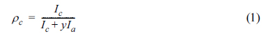
(a) X-ray diffraction patterns of tin oxides obtained from different substrates. A, B, C, and D are the anodized specimens prepared from 1, 20, 100, and 300 ╬╝m-thick tincoated silicon substrates, respectively. E is an anodized specimen prepared from tin foil. (b) Raman spectra of A, D, and E.
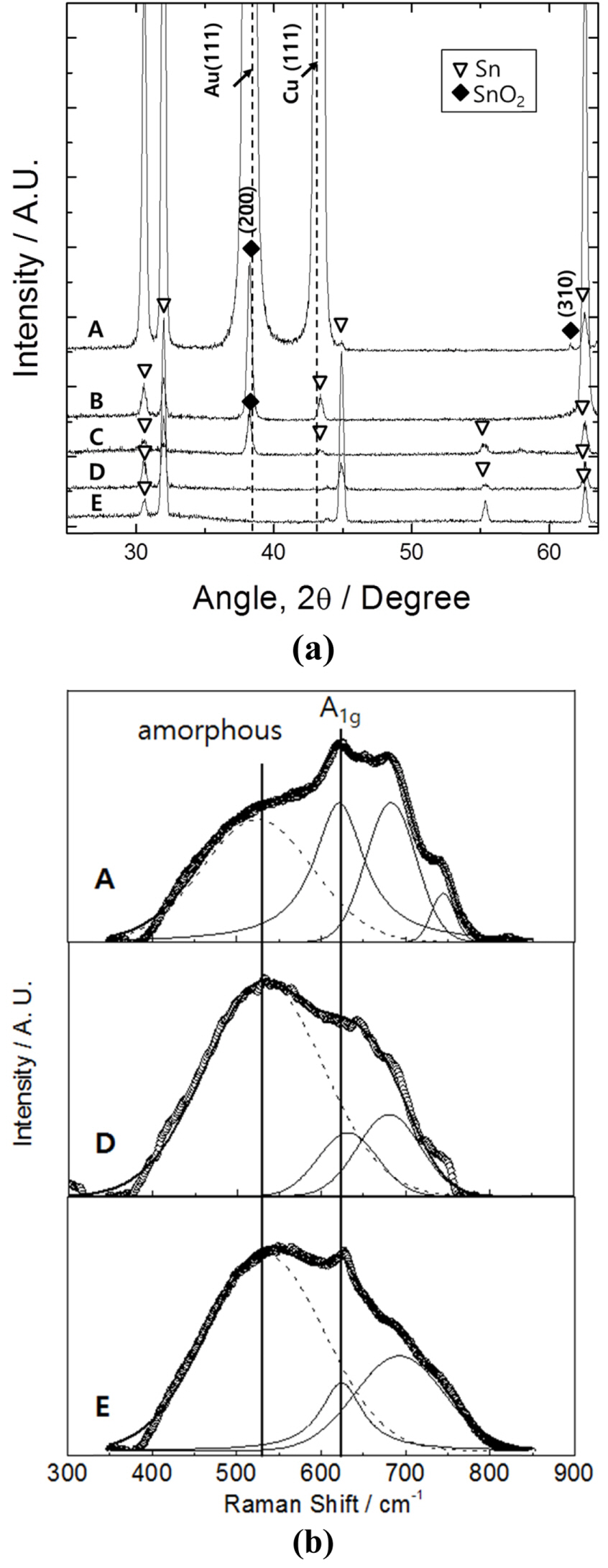
Considering the higher crystallinity obtained with the thinner coatings, the anodic tin oxide formed from 1 ╬╝m-thick-tin-coated silicon is expected to display the most intense SnO2 peak. Unfortunately, it was difficult to clearly distinguish between the signals of the gold layer that is a part of the substrate, and the SnO2 in this specimenŌĆÖs XRD pattern (pattern A in the figure). The signal of the gold layer is completely absent in the case of the 20 ╬╝m-thick tin coating as the signal of the copper layer, which is located on top of the gold, was also absent. Nevertheless, the emergence of an additional SnO2 peak around 61.5┬░ implies it possesses a higher crystallinity than the other samples.
Raman spectra were analyzed to probe the changes in crystallinity more quantitatively, as shown in Fig. 2(b). SnO2 with a tetragonal rutile crystalline structure has 4 Raman-active modes: A1g (631-638 cmŌłÆ1); B1g (100-123 cmŌłÆ1); B2g (770-780 cmŌłÆ1); and Eg (479-480 cmŌłÆ1) [19-24]. Among these, the A1g peak can be used to analyze the degree of crystallinity of SnO2 because its half angle width decreases and its intensity increases with increasing crystallinity [22-24]. In our Raman spectra, the A1g peak is most prominent in the anodic tin oxide formed from the 1 ╬╝m-thick tin coating on silicon. This strongly indicates its higher crystallinity, which was not discernible in the XRD analysis. It is noted that the A1g peak intensity decreased, but was still clearly observed, for the oxides obtained from the 300 ╬╝m-thick tin coating on silicon and from the anodized tin foil. This implies that both samples have some degree of crystallinity though it was undetectable in the XRD analysis.
Another useful measure of tin oxide crystallinity might be the peak that occurs at around 530 cmŌłÆ1. This has been frequently reported, though not clearly assigned [22-24], to be caused by tin oxide with a low degree of crystallinity. As expected, our Raman spectra showed the ~530 cmŌłÆ1 peak intensity was higher for the 300 ╬╝m-thick tin coating on silicon compared to 1 ╬╝m-thick tin coating. Another unassigned peak at 680-690 cmŌłÆ1 in our Raman spectra is known to appear when the crystal grain size is very small (~2-5 nm in diameter) [20].
The following formula was used to calculate the level of crystallinity and to analyze the change in the degree of crystallinity [25,26].
Ic and Ia are the areas of the crystalline and amorphous peaks, respectively. y is the correction factor that is omissible. The A1g peak, the biggest indicator of the degree of crystallinity, was used as the crystalline peak, while the peak at 530 cmŌłÆ1 was used as the amorphous peak. The tin oxide formed by anodizing the 1 ╬╝m-thick tin on silicon has the highest degree of crystallinity at 41.74. In contrast, the anodic tin oxide obtained from the 300 ╬╝m-thick tin coating on silicon has a degree of crystallinity of 13.00, similar to that of the anodized tin foil (14.90). It should be mentioned that the oxide crystallization on the silicon substrate might also be affected by the coating layer (i.e., Ti, Au, and Cu). Particularly, the crystallinity of the tin oxide formed from 1 ╬╝m-thick tin might be most influenced by the coating layer, because the total thickness of the coating layer (~200 nm) relative to the tin film cannot be ignored. This effect needs to be further explored in future work. In summary, the highest degree of crystallinity is acquired when anodizing the 1 ╬╝m-thick tin on silicon, and increasing the tin thickness on silicon substrates results in a lower degree of crystallinity. In particular, the crystallinity of the anodic tin oxide from the 300 ╬╝m-thick tin coating on silicon almost equals that of the anodized tin foil.
The most possible influential factor determining the crystallization of anodized tin oxide might be anodization-induced mechanical stress, as explained by the differing flexibilities of the specimens used in this study. The tin foil is bent away from the side on which the tin oxide forms as the anodization progresses. This is because tin oxide has a larger volume than tin, hence the tin oxide develops tensile stress that causes the highly ductile tin foil to bend. On the other hand, when anodizing the tin-coated silicon, the stress generated cannot be accommodated by deformation of the silicon substrate owing to its high elastic modulus. Therefore, it is expected that a huge compressive stress will be applied to the tin oxide. However, since the surface forming the tin oxide becomes farther from the silicon as the thickness of the tin increases, the thick tin layer between the tin oxide and the silicon is then expected to accommodate, to a certain degree, the stress generated during the oxide formation.
In other words, the compressive stress applied to the tin oxide itself during anodization crucially depends on the mechanical properties of the substrate (ductility or elastic modulus) and the thickness of the tin underneath the anodic oxide layer. Based on the above argument, the difference in crystallinity of the anodic tin oxides observed here can be ascribed to the differences in compressive stress applied to the tin oxide during anodization. Due to this influence, the meager crystallinity of the tin oxide prepared from the tin foil is improved when anodizing tin coated on silicon. Furthermore, the degree of crystallinity increases as the thickness of the tin coating decreases. In fact, phase transition into a crystalline state with small volumes has been reported when a compressive stress is applied to a single-phase amorphous metal [27-31]. Anodic tin oxide is also assumed to follow such a mechanism of crystallization.
To verify whether the above arguments are reasonable, the stress generated from the anodization was experimentally quantified using the Stoney approach [32-34]. The stress applied to the plated layer on the substrate can be calculated from the radius of curvature, R, of the substrate, under the assumption that the specimen is bent by its internal stress. From the measurement of R for the bent specimen and the calculation of the moment about its center, the following equation leads to the internal stress, Žāc, of the coating layer.
E is the YoungŌĆÖs modulus, t is the thickness, and R denotes the radius of curvature of the bent specimen. The subscripts c and s refer to the coating and substrate materials, respectively. When the YoungŌĆÖs modulus of the coating layer and the substrate are different, equation (2) can be rewritten as stated below [33].
Here, E = Ec / Es where Ec is the YoungŌĆÖs modulus of the coating layer, i.e., tin oxide (100 GPa [33]). When the thickness of the coating layer is around 5% of the substrate thickness, the error involved in using StoneyŌĆÖs analysis of equation (3) has been reported to be about 5 to 10 percent, which can be ignored as the experimental error [32]. In this work, we set the tin and anodic tin oxide as the substrate and coating layers, respectively. The thickness of the tin oxide formed after 600 anodization cycles was estimated to be about 1.5 ╬╝m from the SEM observation (inset in Fig. 3). Since this value is about 6% of the substrate thickness (25 ╬╝m), it is assumed that the stress quantification using equation (3) is reliable.
Flexure of the substrate was observed during anodization and its radius of curvature (R) was experimentally measured. At the same time, the change in the tin oxide thickness (tc, inset in Fig. 3) was considered for the calculation of the stress. The radius of curvature decreased and its rate of change slowed down with the number of anodization cycles (or time). The oxide is generated from the tin surface during the early stage of tin oxide formation, thus the substrate bends most during this period. The tin oxide generated thereafter gradually nears the neutral axis of the specimen and does not cause the substrate to bend as much. The decreasing radius of curvature indicates an increase in the tensile force applied to the substrate by the tin oxide. On the other hand, the tin oxide thickness increased linearly with anodizing time (inset in Fig. 3). The tensile stress calculated by equation (3) is presented in Fig. 3. The tensile stress gradually decreases with increasing anodization cycles, indicating that the decrease in the curvature radius, R, is exceeded by the increase in the tin oxide thickness, tc.
Fig.┬Ā3.
Change in curvature radius and stress with the number of anodization cycles, obtained using a tin foil. The inset figure is the change in the thickness of tin oxide during anodization.
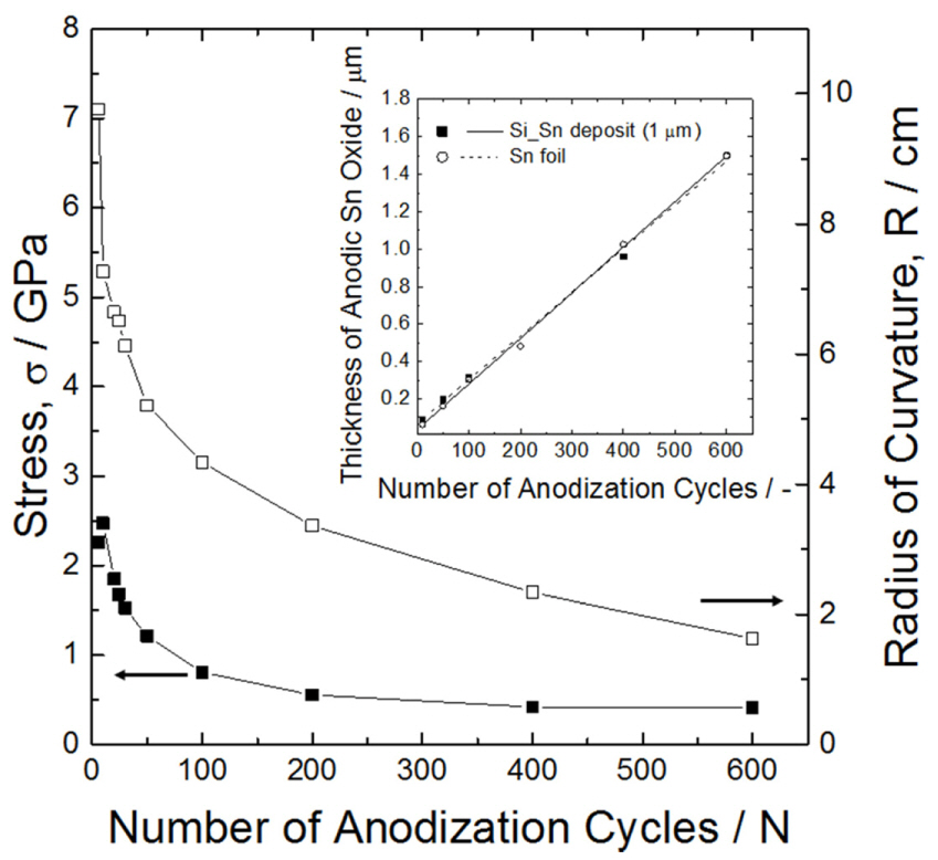
The initial tensile stress triggered by anodic tin oxide formation is about 2.25 GPa, which gradually decreases to a constant value of 0.4 GPa thereafter. Therefore, when anodizing a tin layer coated on a silicon substrate, almost all the stress can be thought of as being accommodated by the oxide without any flexure of the substrate. That is, the same value of compressive stress is seemingly applied to the tin oxide itself.
The crystallization of an amorphous material under compressive stress can be theoretically explained as follows. When a spherical crystalline nucleus with radius r is formed evenly inside an amorphous material under the pressure P, the free energy change can be expressed as shown below [27,28,30,31].
ΔGm is the molar free energy change (i.e., the driving force which triggers the phase transition from amorphous to crystalline), Ee is the elastic energy triggered by the volume change during crystallization,  is the molar volume of the crystal structure, γ is the interfacial free energy between the crystal and amorphous structures, and ΔV is the volume change during formation of the crystalline nucleus. The critical radius for spontaneous growth of the crystalline nucleus, rc, and the corresponding free energy barrier (ΔG*) can be respectively expressed as shown below [30,31].
is the molar volume of the crystal structure, γ is the interfacial free energy between the crystal and amorphous structures, and ΔV is the volume change during formation of the crystalline nucleus. The critical radius for spontaneous growth of the crystalline nucleus, rc, and the corresponding free energy barrier (ΔG*) can be respectively expressed as shown below [30,31].
Since (Ōłé(╬öGm) Ōüä ŌłéP)T = ╬öVm, 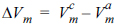 , (where the superscripts c and a refer to the crystalline and amorphous structures, respectively), the change in the free energy barrier caused by the pressure (╬öG*) can be expressed as follows.
, (where the superscripts c and a refer to the crystalline and amorphous structures, respectively), the change in the free energy barrier caused by the pressure (ΔG*) can be expressed as follows.
, (where the superscripts c and a refer to the crystalline and amorphous structures, respectively), the change in the free energy barrier caused by the pressure (ΔG*) can be expressed as follows.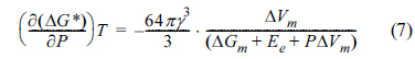
Both ╬öGm and ╬öVm become negative upon transformation from amorphous to crystalline structures, while the change in elastic strain energy (Ee) upon the phase transition is comparatively low [30]. This results in a negative (Ōłé(╬öG*) Ōüä ŌłéP)T value, which indicates that the energy barrier for creating a nucleus of critical size reduces, and the formation of the crystalline nucleus becomes easier with increasing the pressure.
However, when pressure is applied to a material, the energy barrier of atomic diffusion inside the material, Ed, zgenerally increases. Therefore, crystallization under pressure (or stress) involves two contrasting situations: a decrease in the energy barrier for the formation of the crystalline nucleus (ΔG*), and an increase in the energy barrier for atomic diffusion (Ed). It is very challenging to determine the most favorable range of pressures for crystallization by quantifying the ΔG* and Ed under pressure (stress). There have been very few quantitative studies of this relationship in the field of metallurgy [27-31], and we know of no such trials in metal oxides. In this study, the values for an aluminum alloy [30,31] have been used in the calculation to approximate the unknown physical quantities for tin oxide. Consequently, the quantitative interpretations discussed herein are just a rough estimation. Further advancement in the study of accurate physical quantities of tin oxide will enhance the precision of the approach used here.
Ee, ,  , γ, and ΔGm must be assigned for equation (6). The elastic energy (Ee) is calculated from
  , where
 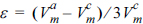 [30,31]. Here, E is the elastic modulus of amorphous tin oxide, which is substituted with the elastic modulus of nanostructured SnO2 (100 GPa [35]). is the volume of crystalline tin oxide, which is 2.15 ├Ś 105 m3/mol, while is assumed to be 2.49 ├Ś 105 m3/mol in reference to the volume ratio of amorphous to crystalline structures reported in metal oxides (approximately 1.16:1.00 [28,30,31]). As there is no reference for the interfacial energy, the existing value found for an aluminum alloy was adopted for convenience (╬│ = 0.1 J/mol [28,30,31]).
, , ╬│, and ╬öGm must be assigned for equation (6). The elastic energy (Ee) is calculated from , where [30,31]. Here, E is the elastic modulus of amorphous tin oxide, which is substituted with the elastic modulus of nanostructured SnO2 (100 GPa [35]). is the volume of crystalline tin oxide, which is 2.15 ├Ś 105 m3/mol, while is assumed to be 2.49 ├Ś 105 m3/mol in reference to the volume ratio of amorphous to crystalline structures reported in metal oxides (approximately 1.16:1.00 [28,30,31]). As there is no reference for the interfacial energy, the existing value found for an aluminum alloy was adopted for convenience (╬│ = 0.1 J/mol [28,30,31]).The free energy barrier in the absence of pressure ( ) can be derived from equation (6) and is presented below.
) can be derived from equation (6) and is presented below.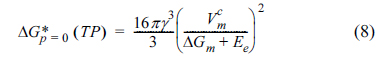
The value of is known to be related to the diffusion energy barrier (ΔEd) and the crystallization energy (Ea), as expressed below [31].
is known to be related to the diffusion energy barrier (ΔEd) and the crystallization energy (Ea), as expressed below [31].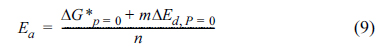
Therefore, upon setting ╬öEd P, = 0 as 146 kJ/mol and Ea as 301 kJ/mol [31], ╬öG*p=0 is calculated to be 766 kJ/mol when a 3-dimensional nucleus is formed (m=3, n=4 [21,36]). Upon substituting this value into equation (8), ╬öGm is calculated to be ŌłÆ5.45 kJ/mol.
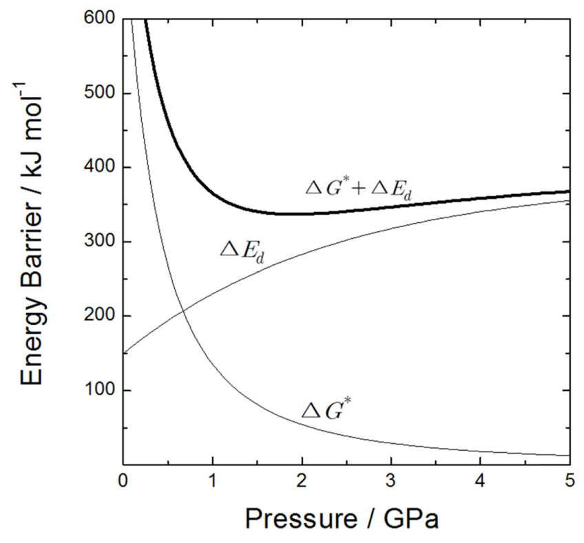
Fig. 4 shows how the free energy barrier for forming the crystalline nucleus changes with pressure, as calculated by substituting the above values into equation (6). Moreover, assuming that ΔEd gradually increases with pressure, ΔG* + ΔEd displays an upward concave shape. In other words, while ΔG* is the dominant factor under relatively low stresses (0-1 GPa), which makes formation of the nucleus more difficult, it rapidly decreases as the pressure increases and ΔEd becomes the dominant factor when the stress is greater than 1 GPa. Therefore, the minimum value of ΔG* + ΔEd and the most favorable conditions for crystallization occur when the stress value is around the minimum (1-2 GPa). Although these calculations are based on various assumptions, the similarity between the experimental compressive stress (0.4-2.25 GPa) that occurs during the formation of the anodized tin oxide and the calculated value of stress at the minimum crystallization energy is very encouraging.
4. Conclusion
This study reported the phenomenon of anodic tin oxide possessing crystallinity and postulated that compressive stress formed inside the tin oxide is the major factor contributing to the crystallization. The deformation of a ductile or easily bent substrate can be used to accommodate the stress caused by the tin oxide. Alternatively, when using a substrate with a high elastic modulus, such as silicon, this mechanism is not feasible and the compressive stress is thus applied to the tin oxide. The stress generated from anodization was measured to be 0.4-2.25 GPa, which closely matches the most favorable theoretical pressure (stress) range for crystallization.


