


1. Introduction
Metal coating on substrates is an important process in the electronics industry. Typical metal coating techniques include chemical vapor deposition (CVD), physical vapor deposition (PVD), metalpowder coating, sputtering, evaporation, and electroless plating [1-5]. Among these, electroless plating, which involves a wet coating, is widely used in the electronics industry due to its simple, inexpensive process, and facile adhesion to the substrate surface. It has been widely used for a long time, especially by manufacturers in the printed circuit board (PCB) industry [6-7]. Recently, metal coatings on polyester fabrics have been investigated as substrates for wearable devices in addition to PCBs and other rigid substrates. Many fabric metal coating methods have been developed, such as the lamination of metal foils, conductive paint coating, sputtering, vacuum evaporation, and flame and arc spraying. However, since these methods are expensive, recent studies have focused on electroless plating methods, which are simple and relatively less expensive [8-15].
The electroless plating process largely consists of three sub-processes: substrate cleaning, seed formation, and electroless plating. In the substrate cleaning process, sulfuric acid is used to clean and remove impurities from the substrate surface to promote seed formation. In the seed formation step, a Pd activator is formed on the surface to catalyze the reduction of Cu2+ ions. The Pd simultaneously facilitates the reduction and promotes the adhesion of the reduced Cu to the surface during the electroless plating process. Therefore, the quality of the metal layer formed by electroless plating is mainly determined by this seed formation process. At present, Sn and Pd are used as activator materials for seed formation. They are both present as ions in solution during the seed formation, and the seeds are formed on the substrate in two steps. First, Pd ions must be reduced to metallic Pd to act as catalysts. Therefore, Sn ions, which can adsorb reducing agents, adhere to the substrate, and Pd ions, which can act as reducing agents, adhere to these Sn ions. Then, Pd forms colloidal particles that adhere to the substrate by oxidation-reduction reactions, and these particles later act as activator during the electroless plating of Cu, Ni, and other metals (Equation 1) [16]. After the formation of the Pd activator, Sn must be removed by adding Cl- ions because they will interfere with the reduction of Cu or Ni later in the electroless plating process. In this way, the activator Pd seed layer is formed on the substrate. This substrate is then immersed in an electroless plating solution to reduce the desired metal ions, and the electroless plating is completed.

Using Pd as an activator for electroless plating is a convenient process, but it has several drawbacks that can give rise to more serious issues. First, the Sn ions must be completely removed by a hydrochloric acid treatment because any residual Sn interferes with the reduction of Cu ions during the subsequent electroless plating. Furthermore, Sn is very toxic and requires specialized waste treatment to prevent environmental pollution. Finally, Pd is very expensive and companies currently using Pd-Sn activators who are dealing with these problems are starting to develop Pd- and Sn-free methods. Dechasit et al. [16] used nickel acetate and cobalt chloride solutions instead of Pd in the seed formation step to form a seed layer on an acrylonitrile-butadiene styrene (ABS) substrate before electroless nickel plating. Garcia et al. [17] modified the substrate surface and grafted poly(acrylic acid) (PAA) onto the surface instead of using a Pd activator, then generated a Cu seed layer for electroless plating by attaching Cu to the end of the PAA branches. Lu [18] treated a polyethylene terephthalate (PET) substrate with silane and used ultrasonication during the electroless plating process. The ultrasonicated PET substrates showed better adhesion and conductivity properties than substrates that did not use ultrasonication. Kaewvilai et al. [19] coated Ag nanoparticles on a glass substrate by dipping it into a silver-benzoxazine solution (AgNO3 and benzoxazine in dichoromethane) and then deposited the copper layer by electroless plating. However, these methods are complex and are difficult for electronics manufacturers to scale up.
Recently, there have been fresh attempts to develop simple and cheap activation processes without Pd-Sn activation by applying copper circuit patterning to flexible devices and wearable electronics. Han et al. [20] transferred Ag from a patterned mask coated with Ag to a PET film using oxygen plasma treatments to form a copper pattern by electroless plating deposition. Lu et al. [21] used a gold nanoparticle solution as a substitute for the Pd-Sn activator for copper conductive pattern fabrication onto paper substrate. They obtained a 2.44 ╬╝m thickness and 6.8 ╬╝╬® cm resistivity for their Cu patterns. Graves et al. [22] used copper nanoparticles as an activator. They dispersed the copper nanoparticles into propan-2-ol using a high-frequency (850 Hz) ultrasonic dispenser for inhibition of agglomeration among copper nanoparticle activators and achieved a very dilute copper nanoparticle suspension (0.01 wt.%).
In this study, Cu electroless plating was performed by first forming a seed layer using Ag nanosol instead of forming an activator layer using Pd and Sn. When the substrate to be plated is first soaked in a diluted Ag nanosol solution and then removed, Ag nanoparticles adhere to the substrate to form a seed layer. Then, the substrate with this Ag seed layer is immersed in a Cu plating solution to perform electroless plating. This Ag-activated Cu electroless plating process has been compared with the conventional process using Pd. The electroless Cu plating method proposed in this study offers several advantages over conventional electroless Cu plating. Specifically, it does not require acid treatment to wash away Sn, which lowers its environmental impact and it does not use expensive Pd.
2. Experimental
2.1. Materials
The sulfuric acid for substrate cleaning was purchased from Daejung Chemical and Material. For the pretreatment solutions, silver nano ink (silver, 60% solids) and isopropyl alcohol (IPA) were purchased from Harima Ink (NPS-J, Japan) and Duksan Pure Chemical, respectively. The silver nano ink used in this study was very diluted. To produce the electroless plating solution, copper (II) sulfate pentahydrate, ethylenediaminetetraacetic acid (EDTA), formaldehyde solution, 2,2'-bipyridyl, and sodium hydroxide were purchased from Kanto Chemical, TCI Chemical, Junsei, Sigma-Aldrich, and Samchun Chemical, respectively.
2.2. Electroless Plating Process
All processes except the electroless plating were performed at room temperature. To clean the substrate before electroless plating, the substrate (FR-4, epoxy line) was soaked in a dilute (5%) sulfuric acid solution for 15 min and then in deionized (DI) water for 5 min followed by drying in air. The nano silver ink consisting of 60% solids was diluted with IPA to a concentration of 0.375 to 3 g/L. The cleaned and dried substrate was pretreated by immersion in the diluted silver sol solution for 10 min before being washed in DI water for 5 min. The silver-pretreated substrate was then immersed in a Cu electroless plating solution at 60┬░C for 1 h to perform the electroless plating. To examine the effects of the silver sol solution pretreatment process on the Cu electroless plating, the Cu electroless plating solution composition and the processing temperature, time, and environment were kept constant. The composition of the electroless plating solution used in this experiment is outlined in Table 1.

Upon completion of the electroless plating process, the substrate was washed with DI water for 10 min and dried in air to produce the final electroless plated substrate.
2.3. Characterization
X-ray photoelectron spectroscopy (XPS, R3000, VG Scienta) was conducted to verify that the silver nanoparticles attached to the substrate after the silver seed layer formation process. Then, X-ray diffraction (XRD, D/MAX-2500, Rigaku Corporation) was conducted to verify the presence of Cu after the electroless plating process. To analyze the surface characteristics according to the concentration of silver nanoparticles and the pretreatment time, a field emission scanning electron microscope (FE-SEM, SU8010, Hitachi) was used. Before the FE-SEM analysis, gold was sputtered onto the specimen using an ion coater (E-1045, Dyeing expert system). To measure the Cu thickness and sheet resistance after electroless plating, an Alpha-Step profilometer (KLA-Tencor) and a four-point probe (MCP-T360, Mitsubishi Chemical) were used, respectively.
A tape test was conducted to test the adhesive strength between the substrate and the Cu layer formed through electroless plating in accordance with the ISO 2409 standard. For this tape test, epoxy substrates were stored for at least 16 h at 23┬░C and 50% relative humidity. A total of 25 squares (1 mm ├Ś 1 mm) were formed by drawing six lines at 1 mm intervals horizontally and vertically. A piece of adhesive tape (3M) was attached to the surface with no gaps. The tape was then removed uniformly at 60┬░, and the condition of the substrate was then examined.
3. Results and Discussion
Fig. 1 shows the transmission electron microscopy (TEM) image and XRD pattern of Ag nanosol used as the activator. As shown in the TEM image of Fig. 1, the silver particles have spherical shape and are approximately 10 nm in diameter. The Ag nanosol was also found to consist of a pure Ag phase without any impurities by XRD.

After the epoxy substrate was pretreated with the diluted silver nanosol solution, which was used in place of a Pd-Sn activator, XPS was conducted to ensure that the Ag nanosol was properly attached to the epoxy substrate. These results are shown in Fig. 2, wherein peaks arising from Ag can be observed at 371, 573, 604, and 1128 eV. This indicates that a seed layer formed easily likely due to the large surface energy of the nanoparticles [23].

A Cu layer was formed by soaking the substrate in a 60┬░C Cu electroless plating solution after pretreating the epoxy substrate with the Ag nanosol. XRD was conducted to verify the formation of the Cu layer after the Cu electroless plating, and the results are shown in Fig. 3. The typical XRD pattern of Cu was observed, with no other peaks indicating the presence of impurities (Fig. 3). The XRD results verified that a Cu layer could be formed on the substrate by reducing Cu ions to metallic Cu through silver nanoparticles attached to the substrate. In the conventional activator formation process, Pd colloids are formed on the substrate surface, and the Cu ions in the plating solution receive electrons from them. The Pd facilitates the reduction and growth of Cu by providing nucleation sites for the Cu reduction reaction and stabilizing the Cu. Then, this newly reduced Cu is surrounded by other Cu ions, and a Cu layer is subsequently formed by self-activation. Likewise, the Ag nanoparticles deposited on the substrate play the same role as Pd by facilitating the reduction of Cu ions and providing nucleation sites.
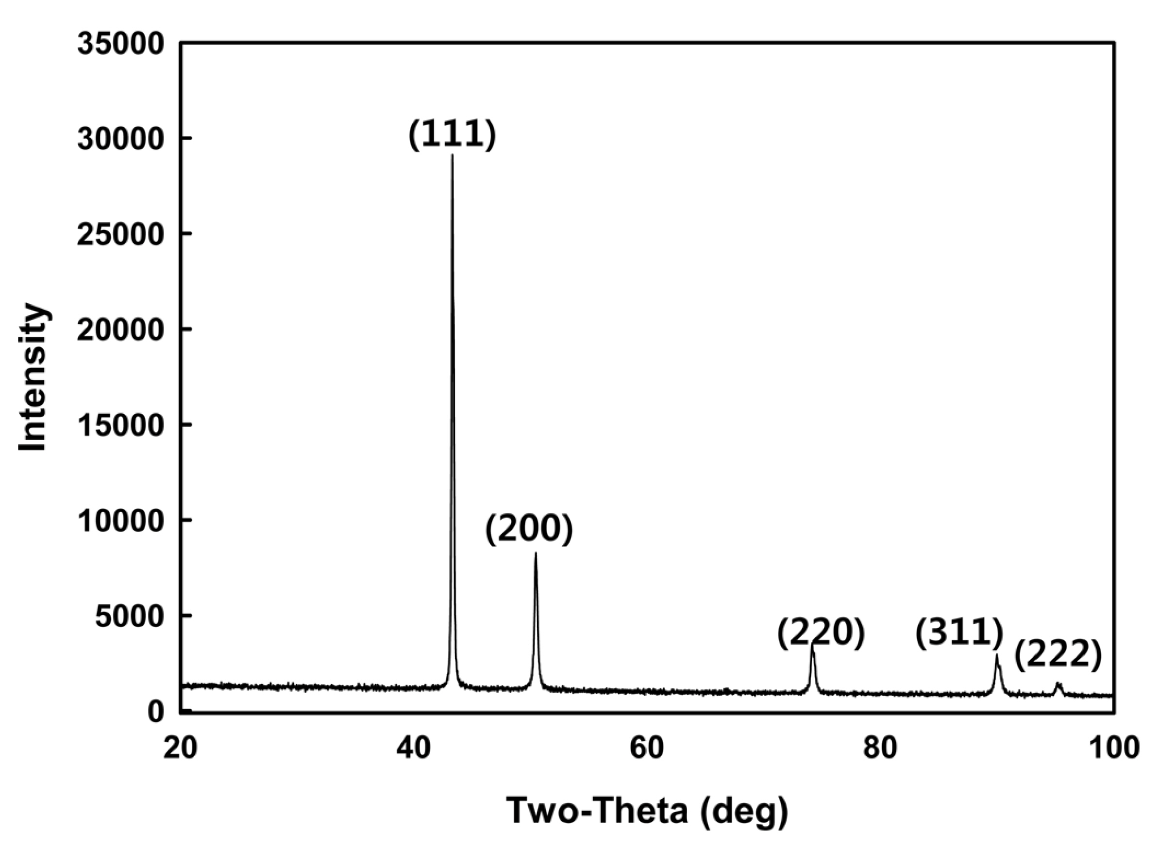
Fig. 4 shows the thickness and sheet resistance with respect to the Ag concentration of the pretreatment solution after 10 min of pretreatment and 1 h of electroless Cu plating. In Fig. 4, the plating thickness increased together with increasing Ag concentration, and the electric resistance decreased accordingly. As the Ag concentration in the pretreatment solution is increased, more Ag seeds are formed on the epoxy substrate, which increased the number of Cu ion reduction sites and accelerated the plating process. Therefore, within the same electroless plating time, the Cu layer on the pretreated substrate becomes thicker with the increasing Ag concentration, and the electric sheet resistance decreases.
Fig.┬Ā4.
Thickness and sheet resistance of the Cu layer according to the concentration of the Ag pretreatment solution after 10 min of pretreatment and 1 h of Cu electroless plating.

A similar trend appeared when the pretreatment time was varied, even with Ag nanosol pretreatment solutions of the same concentration. As shown in Fig. 5, the Cu layer became thicker as the pretreatment time was extended for each Ag nanosol concentration. In particular, the growth rate of the plating thickness gradually increased as the Ag pretreatment concentration became higher. The sheet resistance also decreased as the pretreatment time increased. When the concentration of Ag pretreatment solution was 0.375 g/L, and the pretreatment time was extended from 10 min to 30 min, the sheet resistance of the Cu layer greatly decreased from 0.05 to 0.01 ohm/sq. This indicates that sufficient time to attach Ag nanosol on substrate is needed for optimal Cu plating.
Fig.┬Ā5.
Changes in the thickness and sheet resistance of the Cu layer according to pretreatment time and Ag concentration: (a) thickness and (b) sheet resistance of the Cu layer.

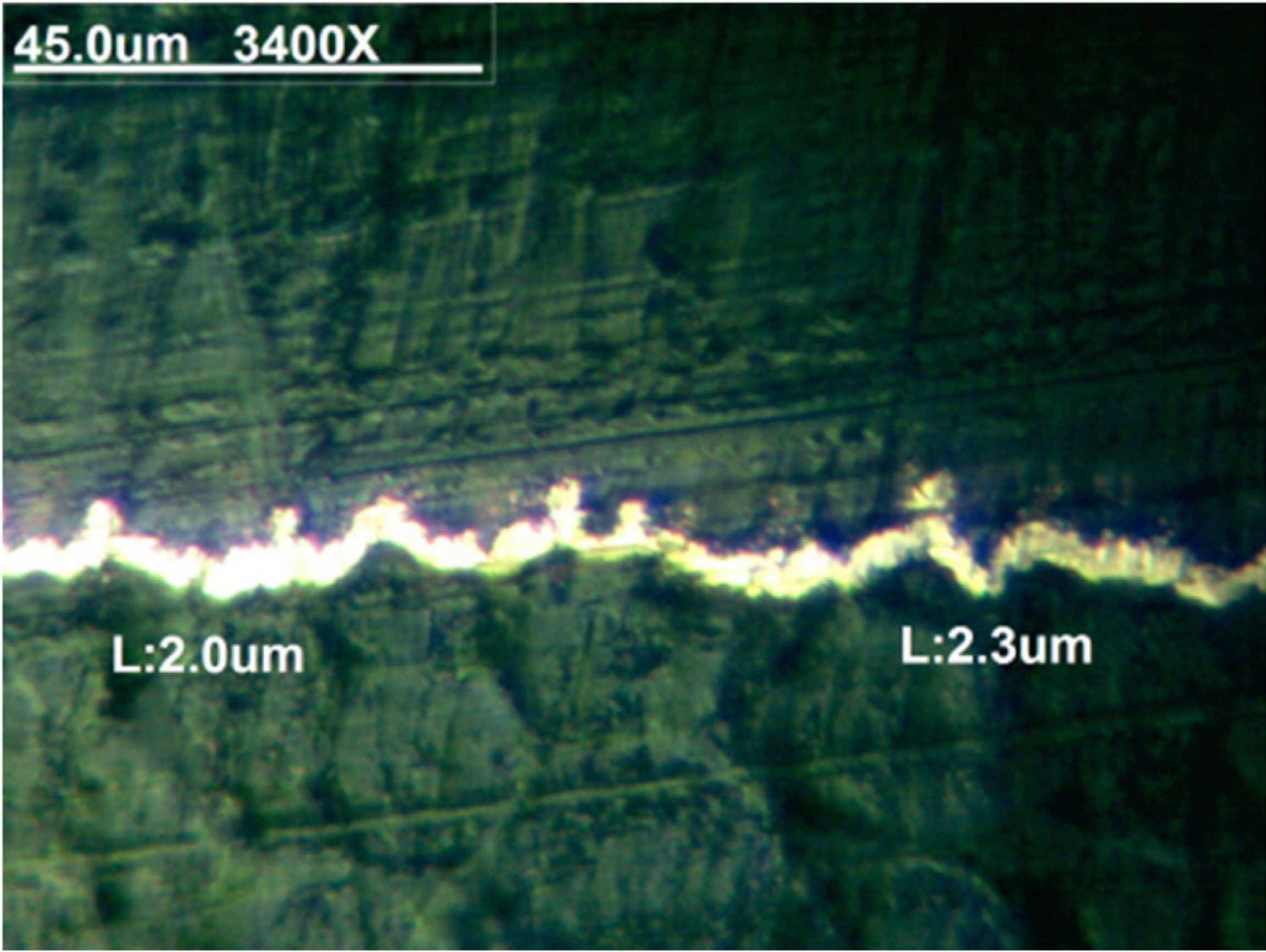
Fig. 6 shows FE-SEM images of the substrate surface after electroless Cu plating with various Ag pretreatment concentrations and times. The Ag pretreatment solution concentrations were 0.375 g/L and 3 g/L, and the pretreatment times were 10 min and 60 min for the plated surfaces observed in Fig. 6. The surface of the bare epoxy substrate with no treatment (Fig. 6(a)) has holes and slight curves. When electroless Cu plating is applied to this epoxy substrate after the Ag pretreatment, the holes and curves in the epoxy substrate are filled with copper, forming a Cu layer with low surface roughness, as shown in Fig. 6 (b)-(e). Similar images can be found in the results of Zhai et al. [24]. They used Cu as an activator on a poly(ether ether ketone) multiwalled carbon nanotube composite substrate for electroless Cu plating. After electroless Cu plating for 40 min, the Cu plated surface was very smooth, independent of initial surface condition of substrate. The copper plated surface exhibited less roughness with 60 min of pretreatment than with 10 min of pretreatment. In addition, the 3 g/L Ag pretreatment solution yielded less surface roughness than the 0.375 g/L solution. This suggests that when the electroless Cu plating creates a thicker Cu layer, the surface of the Cu layer is less affected by the original morphology of the substrate surface. Furthermore, the FE-SEM results verified that the concentration of the Ag pretreatment solution had a greater effect on the thickness of the Cu plating than the pretreatment time. Fig. 7 shows a photograph taken with an optical microscope of a crosssection of the substrate after Ag pretreatment and electroless Cu plating. As shown in Fig. 7, the Cu layer adhered well to the epoxy substrate.
Fig.┬Ā6.
SEM images of the Cu layer surface that had been Cu plated after Ag pretreatment: (a) Bare epoxy, (b) Ag concentration 0.375 g/L, pretreatment time 10 min, (c) Ag concentration 3 g/L, pretreatment time 10 min, (d) Ag concentration 0.375 g/L, pretreatment time 60 min, (e) Ag concentration 3 g/L, pretreatment time 60 min.

Fig.┬Ā7.
A photograph taken with an optical microscope of a cross-section of an epoxy substrate that underwent electroless Cu plating after Ag pretreatment (Ag concentration 3 g/L, pretreatment time 60 min).
Adhesive strength between substrate and Cu layer by electroless plating is important for applications in the electronics industry. The tape test was performed to verify the adhesive strength between the Cu layer and the epoxy substrate in accordance with the ISO 2409 standard. An epoxy substrate that had undergone Cu electroless plating after conventional Pd-Sn pretreatment was also tape-tested for comparison. Fig. 8 shows the results of the tape test for the Cu layers plated after the conventional Pd-Sn pretreatment and the Ag pretreatment. As shown in Fig. 8, the Cu layer did not detach from the epoxy substrate in either case. These results suggest that the pretreatment with the Ag activator forms an equally welladhered Cu layer as the conventional pretreatment with the Pd-Sn activator.

4. Conclusions
A new electroless Cu plating method was developed using Ag nanosol as an activator to improve upon the expense and environmental risk of conventional methods using Pd and Sn. The epoxy substrate was soaked in the Ag pretreatment solution for various times and concentrations before the electroless Cu plating. Higher concentrations and longer pretreatment times resulted in thicker Cu layers and lower the sheet resistance. Furthermore, a cross-cut tape test was conducted to compare the adhesive strength of the Cu layer deposited with the conventional and newly proposed methods. The test results verified that the Cu layer adhered well to the substrate, even when the Ag nanosol was used as an activator, indicating no decrease in the adhesive strength.
This study demonstrated a new electroless plating method which is superior in terms of cost, environmental risk, and simplicity to traditional methods. The proposed method has the potential to replace the use of Pd and Sn in seed layers, which are currently used for electroless plating in the electronics industry.


