1. Introduction
Photoelectrochemical (PEC) water splitting is regarded as an ideal way to generate H
2 energy in an aqueous solution without any external bias using an eco-friendly method. PEC mainly consists of two processes: (1) the hydrogen-evolution reaction (HER) is a relatively rapid process to generate H
2 molecules in a reversible anodic reaction with only two electrons, and (2) the oxygen-evolution reaction (OER), which is a rate-limiting step in which four protons and four electrons from two water molecules participate in bond formation (Žā + ŽĆ of O
2)
[1]. Accordingly, the rate control to catalyze the O-O bond formation is a crucial determinant of the photo-conversion efficiency of water splitting. As a result, the study has been focused on the development and discovery of new photoelectrodes. Usually, metal oxides have been extensively used for photocatalytic and photoelectrochemical hydrogen evolution due to their chemical stability, nontoxicity and relatively low cost
[2,
3]. In particular, since the discovery of catalytic water splitting on TiO
2 photoelectrodes by Fujishima and Honda
[4], considerable efforts have been devoted to developing high efficiency metal oxides in the reaction. However, the large band gap (
Eg) of TiO
2 (> 3.0 eV) limits its light absorption to only 5% of solar light similar to ZnO, Nb
2O
5 and SnO
2. Considering the intimate relationship with photocurrent density and incident solar light absorption in PEC system, the exploration of narrower bandgap materials (e.g., WO
3, ╬▒-Fe
2O
3, BiVO
4) as photoelectrodes is a reasonable approach to enhanced visible light capture
[5-
7]. More recently, copper tungstate (CuWO
4,
Eg = 2.25 eV), which is another material showing visible light absorption to have
n-type behavior, has been actively investigated because of its narrower bandgap relative to that of WO
3 (
Eg = 2.8 eV), the high chemical stability resulting from strong covalency associated with the copper oxygen bonds, inhibition of dissolution to form soluble tungstates by the known acid-base reaction in WO
3 at pH > 5, and high chemoselectivity even in the Cl
ŌłÆ solution
[8]. Furthermore, the edge potential of conduction band is similar to that of WO
3, but the edge potential of valence band is lower than that of WO
3 to approximately 0.5 V
[9]. However, CuWO
4 with poor charge separation efficiency and slow kinetics in the electrolyte interfacial region still exhibits low photoconversion efficiency for OER. Therefore, approaches such as the introduction of effective OER electrocatalyst to minimize the energy penalty associated with water oxidation improved the catalytic efficiency and lowered the excessive potential closely related to the interfacial charge transfer. Specifically, nonprecious and abundant electrocatalysts including Mn-phosphate (MnPO), Co-phosphate, and Ni-based electrocatalysts, have been widely used to reveal the remarkable increase in electrocatalytic properties
[10]. BartlettŌĆÖs group reported that the MnPO-based CuWO
4 photoelectrode exhibited improved PEC performance, corresponding to the cathodic shift of the onset potential for water oxidation by ~ 100 mV and a mild increase in photocurrent density, particularly at low applied bias
[11]. In addition, iron doping or hydrogen treatment of the CuWO
4 film increased the bulk electronic conductivity
[12]. Another strategy involved formation of heterojunctions between CuWO
4 and a second semiconductor, such as WO
3, BiVO
4, and Ag
2NCN with synergetic enhancement in photocurrent density. AdamŌĆÖs group used Ag
2NCN to functionalize the CuWO
4 surface resulting in 3-fold increase in photocurrent density, attributed to more efficient charge separation and hole collection efficiencies under circumstances where the higher position of conduction band edge of Ag
2NCN favored charge carrier separation at the interface
[13]. Similarly, the WO
3/CuWO
4 photo-anodes show effective band alignment for charge separation from the conduction band edge of WO
3 to CuWO
4 resulting in higher photocurrent.
Recently, we reported the photoelectrochemical behavior based on a WO
3-coated fluorine-doped SnO
2 (FTO) inverse opal (IO) nanostructure
[14]. An electrodeposited WO
3 film was uniformly coated on the FTO inverse opal template using electrodeposition, contributing to enhanced visible-light absorption resulting in the best photocurrent of 2.9 mA/cm
2. FTO takes part in a good electronic conducting skeleton to show semi-metallic property, enabling favorable charge transport in a non-conductive semiconductor photoanode. Further, the 3-dimensional (3D) inverse opal provides sufficient surface area for the PEC reaction, intensifying the light absorption by the photonic crystal effect. Therefore, in the present study, the CuWO
4 showing narrower band gap and strong chemical stability relative to that of WO
3 was deposited on the FTO inverse opal, directly mediating the PEC reaction, using a facile electrodeposition. According to the number of cycles in the cyclic voltammetry of a specific potential range, the electrodeposited CuWO
4 thickness was modulated, suggesting that 4 cycles yielded the optimum photocurrent density. The CuWO
4 nanoparticles covered the entire FTO IO film sparsely, contributing to enhanced visible light absorption as well as retardation in charge recombination and dramatic reduction in interfacial resistance. The development and related characterization based on the FTO/CuWO
4 IO films are discussed.
3. Results and Discussion
Fig. 1 represents the high resolution FE-SEM images of the hexagonally aligned FTO, FTO/CuWO
4(4 cycles), and FTO/CuWO
4(8 cycles) films. Generally, the IO films exhibit honeycomb-shaped hexagonal close-packed array, dense coverage and crack-free structure. Compared with the diameter 410 (┬▒ 5) nm of the pristine multilayered PS template arranged in a regular array of close-packed and layered colloids, the pore diameter of IOs was decreased to approximately 300 nm and the pore shrinkage of about 27% probably due to the loss of liquid volume from the precursor and the densification of FTO during the phase transformation from the amorphous to the rutile phase. This shrinkage was similar to the previous case (25-30%) captured from the sol-gel based structure
[17]. The wall thickness between each micropore was ~20 nm (┬▒ 5) nm with thicker walls at the contact area and the length of the prepared FTO IO was approximately 3.7 ╬╝m. A thin CuWO
4 layer was coated on the FTO IO films by facile electrodeposition using cyclic voltammetry, altering the number of cycles from 4 cycles (
Fig. 1(b)) to 8 cycles (
Fig. 1(c)). Both FTO/CuWO
4 IO films showed distribution of partially agglomerated CuWO
4 nanoparticles through the entire FTO IO surface with a higher density in the FTO/CuWO
4(8 cycles) IO film. This result indicates that the increased cycling induced further deposition of CuWO
4 layer, although the relation was not directly linear. Hence, it is apparent that the pore diameter was slightly reduced to approximately 10 nm and the wall thickness was irregularly decreased or increased depending on the presence of CuWO
4 nanoparticles in well-ordered hexagonal-close packed arrangement of the FTO IO skeleton. To confirm the uniformity of the electrodeposited CuWO
4 layer and thickness in the FTO IO films, the cross-sectional images of FTO and FTO/CuWO
4(4 cycles) IOs films were measured, as illustrated in the inset of
Fig. 1(b). Both samples exhibit a similar thickness of 3.1 ╬╝m, disclosing the partial coating of CuWO
4 layer into the interior FTO IO films.
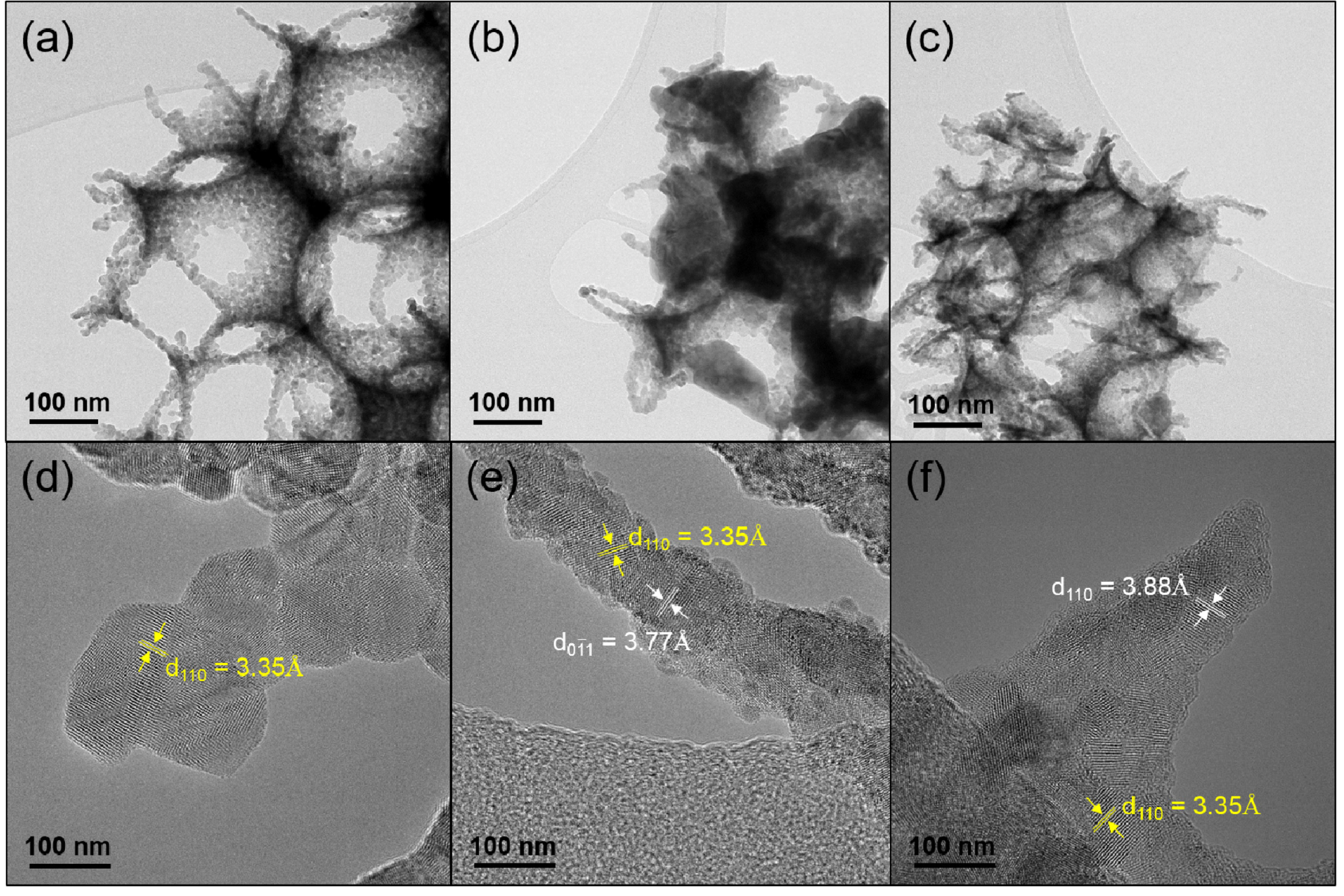
To further survey the morphology and crystalline properties of the IO films, the TEM measurements were performed, as presented in
Fig. 2. Herein, the FTO and FTO/CuWO
4 IO films were prepared for a comparison. In the case of FTO IO film, an assembly of the extremely small crystallites of FTO with an average size of ~ 5 nm was comprised of 3D ordered macroporous IO structure because the FTO IO film was prepared by the sol-gel assisted spin coating method. The pore size of FTO IO film exists in ~ 300 nm to be identical to the image captured from FE-SEM (
Fig. 1). Furthermore, to certify the crystallinity of the FTO IO film, the TEM image measured in HR-mode was shown in
Fig. 2(d), revealing an inter-planar lattice spacing of 3.35 ├ģ with clear lattice fringes which conforms to the rutile (110) plane of the SnO
2 crystal system. In the case of FTO/CuWO
4(4cycles) IO film in
Fig. 2(b), the less porous IO structure was observed and partially agglomerated owing to the thick CuWO
4 coating, attributed from the electrode-position in the repetitively cycling of potential in which the CuWO
4 nanoparticles on the vicinity of the initial seed layer formed on the surface of FTO IO can grow quite fast and the uneven coverage via the surface of FTO IO film happened. Also, the crystalline (110) and (0-11) planes from FTO and CuWO
4 phase (
Fig. 2(e)) were clearly observed from an interplanar lattice spacing of 3.35 ├ģ and 3.77 ├ģ with clear lattice fringes, respectively, which complies with the rutile and triclinic plane of SnO
2 and CuWO
4 crystal system
[18]. Fortunately, the FTO as well as the CuWO
4 phases were concurrently found to confirm the crystallinity of the FTO/CuWO
4(4cycles) IO films. In the case of FTO/CuWO
4(8cycles) IO film in
Fig. 2(c and
f), the more agglomerated CuWO
4 layer on FTO IO film was observed due to the more cycling in the same potential range, further disclosing an inter-planar lattice spacing of 3.35 ├ģ and 3.88 ├ģ with clear lattice fringes which are consistent with the rutile (110) plane and triclinic (110) plane of SnO
2 and CuWO
4 crystal system.To verify the crystalline properties of FTO, FTO/CuWO
4(4cycles), and FTO/CuWO
4(8 cycles) IO films, XRD analysis was performed and the results are shown in
Fig. 3. All the diffraction peaks in the FTO IO-based samples were indexed to the tetragonal phase of SnO
2 (JCPDS no. 41-1445; a = 4.7 ├ģ, c = 3.2 ├ģ) corresponding to (110), (101), (200) and (211) reflections at 26.5┬░, 33.8┬░, 37.8┬░ and 51.7┬░, respectively, even though the 10 wt % F
ŌłÆ ions were doped in the main SnO
2 material. In the case of FTO/CuWO
4 IO films, additional triclinic CuWO
4 peaks (JCPDF no: 73-1823) with the representative (110), (0-10), (100) and (021) planes at 23.01┬░, 23.57┬░, 24.24┬░ and 33.21┬░ were remarkably obtained with a lattice parameter of
a = 4.71 ├ģ,
b = 4.88 ├ģ and
c = 5.84 ├ģ, which was consistent with the preceding literature
[18], together with the rutile FTO peaks. In addition, no additional peaks, establishing the absence of other crystallites or impurities such as SnO
x and WO
x were observed. Furthermore, based on ScherrerŌĆÖs equation, the average crystallite size of each sample was calculated using the main (100) plane from CuWO
4 phase to yield an average grain size of 21.57 nm in 4 and 8 cycles of FTO/CuWO
4 IO films, reflecting the absence of further growth of CuWO
4 nanoparticles during the cycling of potential.
Fig.┬Ā1.
Surface FE-SEM images of (a) FTO, (b) FTO/CuWO4(4cycles) and (c) FTO/CuWO4(8 cycles) IO films.

Fig.┬Ā2.
Low magnification TEM images of (a) FTO, (b) FTO/CuWO4(4cycles) and (c) FTO/CuWO4(8 cycles) IO films. High-magnification TEM images of (c) FTO, (d) FTO/CuWO4(4cycles) and (f) FTO/CuWO4(8 cycles) IO films.

Fig.┬Ā3.
Typical XRD patterns of (a) FTO, (b) FTO/CuWO4(4cycles) and (c) FTO/CuWO4(8 cycles) IO films.

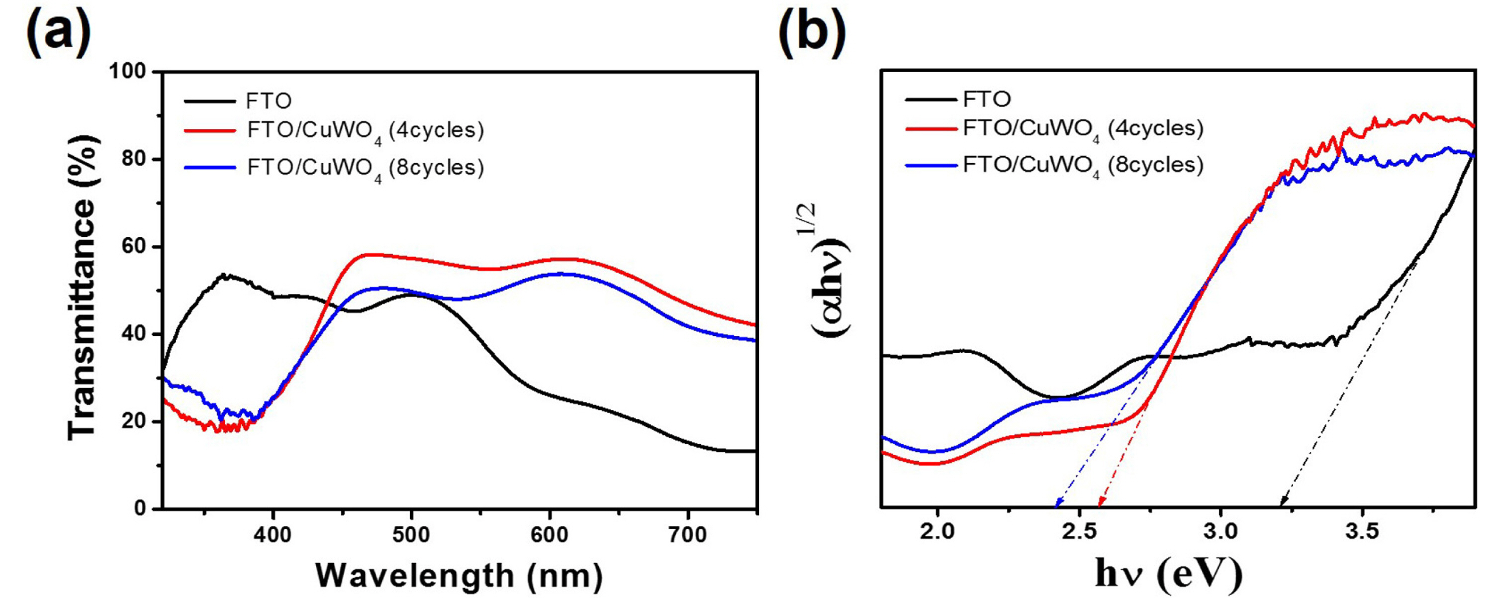
Fig. 4 depicts the UV-vis transmittance spectra of the FTO, FTO/CuWO
4(4 cycles) and FTO/CuWO
4(8 cycles) IO films developed on the FTO substrate. The absorption onset for FTO IO was ~ 360 nm, suggesting a UV-active material. On the other hand, it was well known that the CuWO
4 shows an indirect band gap due to the absence of sharp absorption, in that the absorptivity coefficient,
a, was 6600 cm
ŌłÆ1 at 400 nm, which sharply decreased to 1715 cm
ŌłÆ1 at 500 nm
[16]. Although the CuWO
4 exhibited an indirect band gap, it may still result in high photoactivity with nanowire or nanoplatelet morphologies as well as modified charge transport pathways following introduction of other materials. In this study, the absorption onset of FTO/CuWO
4 IO film was ~ 470 nm with enhanced light absorption toward visible wavelength. The high transmittance in FTO/CuWO
4(4 cycles) IO film indirectly reflects the contribution of increased light absorption corresponding to a little scattering and reflection, compared with that of FTO/CuWO
4(8 cycles) IO film in the identical structure. A minor fluctuating absorption band above 500 nm may result from the photonic crystal effect in the 3D inverse opal structure. The precise optical bandgap (
Eg) of all samples was calculated by extrapolating the linear portion of the (╬▒h╬Į)
1/2 vs h╬Į plot, known as Tauc plot, displayed in
Fig. 4(b), where
╬▒ represents absorption coefficient and h╬Į is the incident photon energy. The estimated
Eg of FTO, FTO/CuWO
4(4 cycles) and FTO/CuWO
4(8 cycles) IO films were 3.55 eV, 2.57 eV, and 2.42 eV, respectively. It has been reported that the original CuWO
4 band gap was approximately 2.2 eV. However, increasing the cycle number in cyclic voltammetry elevated the loading amount of CuWO
4 layer. Considering that the light recognizes the combined FTO and CuWO
4 layers in 3D inverse opal structure, the
Eg of FTO/CuWO
4(8 cycles) IO film was shifted to a lower band gap, relative to that of 4 cycles, to approach the original band gap of CuWO
4. Perhaps, as the loading amount of CuWO
4 on the FTO IO film increased further, the total bandgap was decided by the deposited CuWO
4 layer to reach to the bandgap of 2.2 eV.
Fig.┬Ā4.
(a) UV-vis transmittance spectra and (b) Tauc plot of FTO, FTO/CuWO4(4cycles) and FTO/CuWO4(8 cycles) IO films.

To identify the PEC behavior of FTO and FTO/CuWO
4 IO films, the fundamental PEC properties were characterized as shown in
Fig. 5.
Fig. 5(a) shows a set of linear sweep voltammetry of FTO, FTO/CuWO
4(4 cycles) and FTO/CuWO
4(8 cycles) IO films under chopped illumination (AM 1.5G, 100 mW/cm
2) in 0.5 M Na
2SO
4 (pH 6.5). Considering that the dark current acquired under dark was in the range of ~ 10
ŌłÆ2 mA/cm
2, the photoresponse of all the samples was remarkably under light illumination. Furthermore, the prompt photoresponse of the samples indicates general stability of the photocurrents without photo-induced charging effects. FTO IO film exhibited a photocurrent density (J
sc) of 0.14 mA/cm
2 at 1.23 V
RHE, whilst the substantially larger photocurrent densities were achieved by the FTO/CuWO
4(4 cycles) with a J
sc of 0.42 mA/cm
2, followed by the FTO/CuWO
4(8 cycles) possessing a J
sc of 0.24 mA/cm
2 at 1.23 V
RHE. Compared with the FTO IO film, the FTO/CuWO
4(4 cycles) IO films attained approximately 3-fold enhancement emphasizing the positive role of heterojunction FTO-CuWO
4 combination as a core-shell structure improving the photoactivity of FTO or CuWO
4 film under illumination. This photocurrent densities is a little bit lower that the recently reported the highest value (0.58 mA/cm
2 at 0.8 V V
RHE) and exist in the meaningful value
[19]. However, increasing the amount of CuWO
4 loading reversibly, the J
sc was rapidly degraded, probably due to the mechanically unstable contact between FTO IO and CuWO
4 layers, resulting in rapid charge recombination. Furthermore, the modification of FTO IO structure with a CuWO
4 layer resulted in the anodic shift of the onset potential by ca. 150 mV, compared with (0.36 V) observed for the base FTO IO electrode (not shown here). However, the magnitude of the photocurrent was extremely low and possibly lost in the background signal due to the high overpotential in this region. As a control sample, the CuWO
4 film on the FTO substrate was also grown under the same experimental condition, showing no photoresponse in the entire potential range (not shown here). To intimately examine the photoresponse under visible light from the CuWO
4 layer with an
Eg of approximately 2.5 eV, the chopped on/off LSVs were again measured using a 400 nm cutoff filter and the results are presented in
Figure 5(b). Unexpectedly, a significant J
sc (0.1 mA/cm
2 at 1.23 V
RHE) from the CuWO
4 layer (4 cycles) was achieved under visible light coinciding with the sequence obtained from the LSVs under full solar illumination. Further CuWO
4 layer (8 cycles) also showed the degradation of J
sc under visible light.
To review the generation of photocurrent density, IPCE measurements were carried out at 1.0 V vs RHE in the 0.5 M Na
2SO
4 solution, as depicted in
Fig. 5(c). The FTO IO film showed the typical photoresponse of FTO material corresponding to a maximum IPCE of 3.42% at 315 nm and an onset potential of 385 nm. Furthermore, the FTO/CuWO
4 IO films exhibit two distinct peaks from the respective FTO and CuWO
4 layers and have identical overall IPCE patterns. In the case of FTO/CuWO
4(4 cycles), the maximum IPCE value of 9.4% was obtained at 315 nm with a broad shoulder peak caused by the CuWO
4 layer, corresponding to an IPCE value of 7.45% at 390 nm, whereas the FTO/CuWO
4(8 cycles) shows the maximum IPCE value of 5.89% at 315 nm with the IPCE shoulder peak of 4.17% at 390 nm. The onset wavelength of FTO/CuWO
4 IO films exists in the same wavelength of 475 nm due to the light absorption of the CuWO
4 layer. In general, the IPCE is obtained by the following equation
[20]:
where
J denotes the measured photocurrent density at a specific wavelength;
╬╗ is the wavelength of incident light; and
Jlight stands for the measured irradiance at a specific wavelength. The J
sc calculated by the integration of each IPCE spectrum was similar to J
sc at 1.0 V vs. RHE in
Fig. 5(a). As a whole, the FTO/CuWO
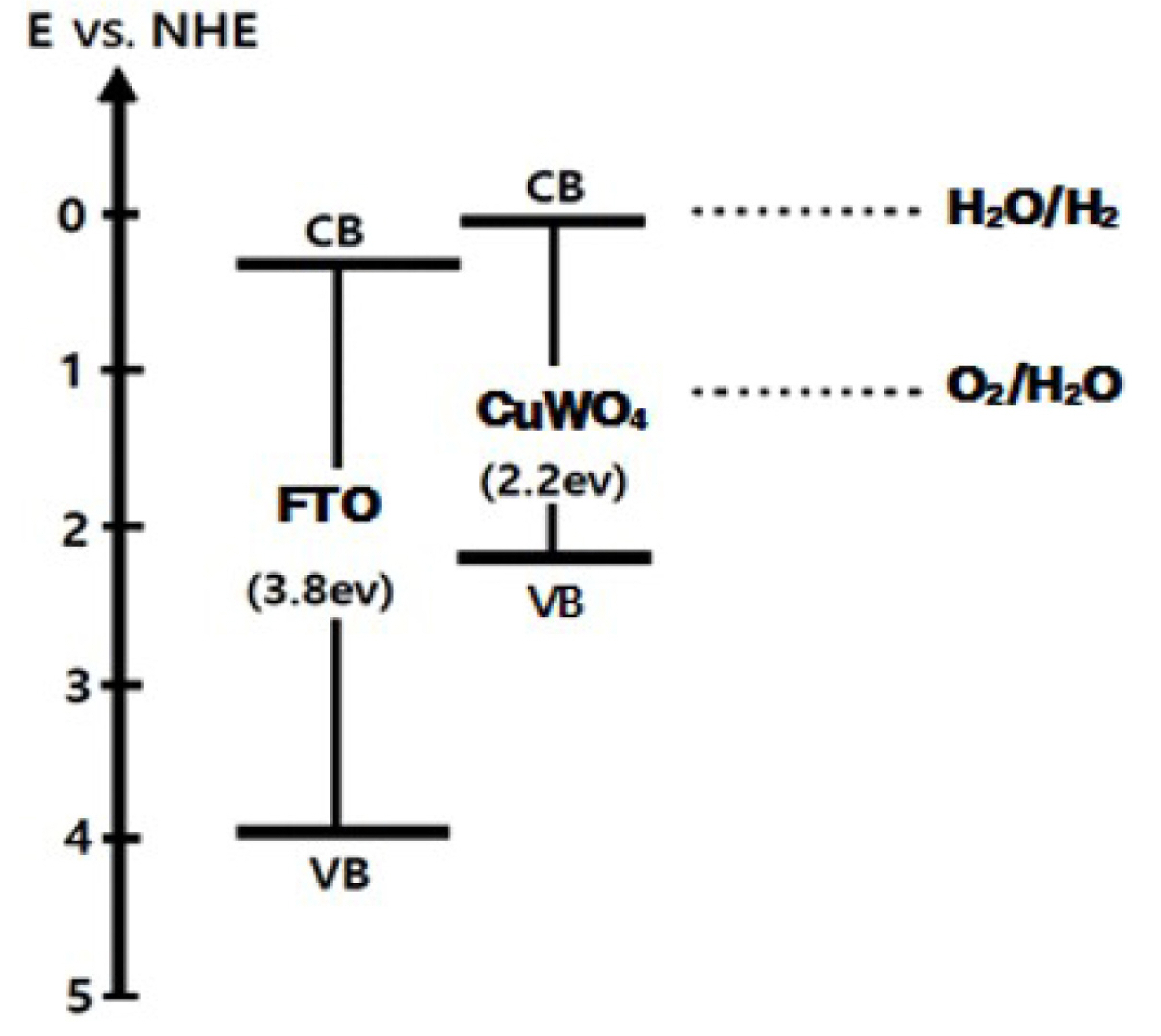
4(4 cycles) film exhibits substantially enhanced photoactivity over the entire UV and near visible region, attributed to electrically conducting FTO core IO as well as the visible light absorbing CuWO
4 shell layer under the favorably cascading band alignment between the FTO and CuWO
4 materials.
To determine the electrochemical kinetics at each component and interfacial region in the PEC system, the EIS analysis was conducted at the frequency range of 10 kHz to 0.1 Hz at OCV under solar illumination.
Fig. 5(d) shows the Nyquist plots of the FTO and FTO/CuWO
4 IO films in the 0.1 M Na
2SO
4 solution including the suggested equivalent circuit for the simulation to obtain the exact and quantitative fitted values from each component, including R
s indicating the ohmic or series resistance including the FTO substrate, the resistance associated with the ionic conductivity in the electrolyte and the external contact resistance at the high frequency. R
ct in the low and middle frequency is correlated with the semiconductor/electrolyte charge transfer resistance. Furthermore, the constant phase element (CPE) represents the non-ideal capacitance of the Helmholtz layer in the nanoporous semiconductor/electrolyte interface
[21]. The quantitatively fitted data are summarized in
Table 1. All samples exhibited a similar value of ~ 220 ╬®, suggesting that all samples existed in the analog environment. Meanwhile, FTO IO showed significantly high R
ct of approximately 18890 ╬®, whereas FTO/CuWO
4 IO films exhibited quite low R
ct values of 8000-10000 ╬®, indicating that the photogenerated holes in the FTO IO film experience more than twice the magnitude of difficulty to reach the electrolyte compared with the FTO/CuWO
4(4 cycles) IO film. The introduction of CuWO
4 layer on the FTO IO film passivates the surface state or trap sites in the surface region of FTO IO film, promoting rapid charge transfer in the solid-liquid interface, which induces a low R
ct and finally, contributes to the enhanced PEC activity.
Fig.┬Ā5.
(a) Chopped LSV under full sun on/off cycles, (b) Chopped LSV under visible sun on/off cycles (c) IPCE spectra of FTO and FTO/CuWO4 IO films in 0.5 M Na2SO4 solution, and (d) EIS spectra under solar illumination in FTO and FTO/CuWO4 IO films including the electrical equivalent circuit in the inset of (d).

Table┬Ā1.
Quantitative values of ohmic resistance (Rs) and charge-transfer resistance (Rct) of FTO and FTO/CuWO4 IO films fitted using the suggested equivalent electrical circuit.

In summary, the electrodeposition of thin CuWO
4 layer on the FTO IO film was successfully developed using cyclic voltammetry by varying the cycling number from 4 to 8 cycles. FTO/CuWO
4(4 cycles) IO film exhibited the highest J
sc (0.42 mA/cm
2 at 1.23 V
RHE), while FTO IO film showed a J
sc of 0.14 mA/cm
2 at 1.23 V
RHE. The FTO/CuWO
4 (8 cycles) IO film displays a J
sc of 0.24 mA/cm
2 at 1.23 V
RHE. An approximately 3-fold enhancement of J
sc was attained in the deposition of the optimum CuWO
4 layer on FTO IO film, attributed to improved visible light absorption and favorable band alignment between CuWO
4 and FTO materials (
Fig. 6), accelerating the charge separation and charge transfer rate in the solid/liquid junction. On the other hand, the thick and denser CuWO
4 loading on the FTO IO film induced mechanically brittle connection, reversibly increasing the charge recombination reaction, resulting in the degradation of PEC performance.
Fig.┬Ā6.
Schematic cascade of band alignment between FTO and CuWO4 materials to show the beneficial charge transfer events.
