 |
 |
- Search
| J. Electrochem. Sci. Technol > Volume 10(4); 2019 > Article |
|
Abstract
Planar BiVO4 and 3 wt% Mo-doped BiVO4 (abbreviated as Mo:BiVO4) film were prepared by the facile spin-coating method on fluorine doped SnO2(FTO) substrate in the same precursor solution including the Mo precursor in Mo:BiVO4 film. After annealing at a high temperature of 450°C for 30 min to improve crystallinity, the films exhibited the monoclinic crystalline phase and nanoporous architecture. Both films showed no remarkably discrepancy in crystalline or morphological properties. To investigate the effect of surface passivation exploring the Al2O3 layer, the ultra-thin Al2O3 layer with a thickness of approximately 2 nm was deposited on BiVO4 film using the atomic layer deposition (ALD) method. No distinct morphological modification was observed for all prepared BiVO4 and Mo:BiVO4 films. Only slightly reduced nanopores were observed. Although both samples showed some reduction of light absorption in the visible wavelength after coating of Al2O3 layer, the Al2O3 coated BiVO4 (Al2O3/BiVO4) film exhibited enhanced photoelectrochemical performance in 0.5 M Na2SO4 solution (pH 6.5), having higher photocurrent density (0.91 mA/cm2 at 1.23 V vs. reversible hydrogen electrode (RHE), briefly abbreviated as VRHE) than BiVO4 film (0.12 mA/cm2 at 1.23 VRHE). Moreover, Al2O3 coating on the Mo:BiVO4 film exhibited more enhanced photocurrent density (1.5 mA/cm2 at 1.23 VRHE) than the Mo:BiVO4 film (0.86 mA/cm2 at 1.23 VRHE). To examine the reasons, capacitance measurement and Mott-Schottky analysis were conducted, revealing that the significant degradation of capacitance value was observed in both BiVO4 film and Al2O3/Mo:BiVO4 film, probably due to degraded capacitance by surface passivation. Furthermore, the flat-band potential (VFB) was negatively shifted to about 200 mV while the electronic conductivities were enhanced by Al2O3 coating in both samples, contributing to the advancement of PEC performance by ultra-thin Al2O3 layer.
Photoelectrochemical (PEC) water splitting using solar light source and proper semiconductor photoelectrode has been considered a sustainable hydrogen production method. To develop a high-performance photoanode for water oxidation, half reaction under visible light, a semiconductor with a suitable band gap (1.9 eV < Eg < 3.1 eV), and a proper position of band gap decorated with a thin layer of water oxidation cocatalyst are required [1,2]. As a representative, BiVO4 (Eg = 2.4 eV) has emerged as one of the most promising photoanode materials to absorb more visible light with proper band position to evolve the hydrogen and oxygen from water photoelectrolysis and excellent stability of the liquid-solid interface [3,4]. Based on band gap of 2.4 eV, the theoretical maximum photocurrent of ~7.5 mA/cm2 at one sun irradiation can be achieved [5]. However, most of BiVO4 films still exhibit quite low PEC performance. The main reasons can be explained by an inefficient charge separation at the interface and unfavorable charge transportation through the photoelectrode, leading to the low photocurrent density in PEC working condition [6]. Thus, the heterojunction composed of the core and shell layer showing good band alignment could potentially cope with these weak points of BiVO4 material. As a recent representative example, 1D cobalt-phosphate (Co-Pi) modified BiVO4/ZnO junction showing cascading band alignment has exhibited a photocurrent of ~3 mA/cm2 at the highest photocurrent density [7]. This is probably due to enhanced visible light absorption and fast electron transport along 1D ZnO nanorods. Also, controlled growth of BiVO4 layer on the inverse opal WO3 photoanodes has been fabricated by a template-assisted route to form the heterojunction of the WO3/BiVO4 layer [8]. In the similar viewpoint, ultra-thin passivation layers have also been introduced on BiVO4 photoanode as the blocking layer against charge recombination reaction and the photocorrosion [9]. Several materials have been already investigated, including TiO2, NiOx, CoOx, and Al2O3 [10–13]. Lewis et al. have reported that ultra-thin amorphous TiO2 layers with a thickness of ~1 nm can suppress the photocorrosion, revealing a stable photocurrent of ~1.4 mA/cm2 at 1.23 VRHE under one sun irradiation during the testing of several hours [14]. Domen et al. have found that ultra-thin NiOx layers with a thickness of ~6 nm can enhance PEC performance as well as photostability in CoOx−coated BiVO4 film, achieving solar-to-hydrogen efficiency of ~1.5% [15]. Kafizas et al. have investigated the effect of ultra-thin Al2O3 layer with an optimum thickness of approximately 0.33 nm, displaying a remarkable increase in theoretical solar photocurrent from ~0.47 mA/cm2 (uncoated BiVO4 film) to ~3.0 mA/cm2 (Al2O3/ BiVO4 film) , due to suppression of charge recombination reaction [16]. However, in this paper, there is no report on the doped BiVO4 film which shows the more efficient PEC performance. Even though the surface state of pristine and doped BiVO4 film is somewhat different, it can be expected that the introduction of ultra-thin Al2O3 layer on the doped BiVO4 film can contribute to the efficient photoelectrochemical activity.
Accordingly, we investigated the role of ultra-thin Al2O3 layer on the undoped and Mo-doped BiVO4 (briefly abbreviated as Mo:BiVO4) film and their PEC behavior was studied in detail. The Al2O3 layer with a thickness of approximately 2 nm was prepared on the BiVO4 and Mo:BiVO4 films by the atomic layer deposition (ALD) process and the effectiveness of surface passivation on undoped and doped BiVO4 films was compared using several analyses tools. Al2O3/Mo:BiVO4 films exhibited enhanced PEC performance, having a photocurrent of 1.5 mA/cm2 at 1.23 VRHE compared to Mo:BiVO4 film (0.91 mA/cm2). Similarly, the Al2O3/BiVO4 film exhibited improved photocurrent density of 0.86 mA/cm2 at 1.23 VRHE, relative to BiVO4 film (0.12 mA/cm2). This may be due to the favorable charge transfer/transportation in the Mo:BiVO4 film as well as the degraded charge recombination. Above different films, when cobalt-phosphate (Co-Pi) as a cocatalyst was covered on the top of the film, the maximum photocurrent density of 1.85 mA/cm2 at 1.23 VRHE was obtained.
An FTO (Pilkington TEC GlassTM, sheet resistance 8 Ω sq−1) as a substrate was prepared by following a cleaning process in deionized (DI) water, ethanol, and acetone for 20 min in each step to remove some organic contamination and dust. For spin-coating to make undoped BiVO4 film, precursors composed of 0.2M ammonium metavanadate in 5 mL deionized (DI) water and 5 mL 60 wt% HNO3 solution were mixed and stirred continuously until turning to a transparent solution. Then 0.2M bismuth nitrate in 10 mL methanol was added to complete the BiVO4 solution. Prior to spin coating, the prepared solution was aged for one day. The spin-coating (a volume of 50 μL) was performed under 1500 rpm for 20 sec to make a BiVO4 film. In the case of 3 wt% Mo:BiVO4 film, the composition of the prepared solution was the same as BiVO4 except that 3 wt% sodium molybdate as an additional source material was added into the solution. The deposition procedure to make the Mo:BiVO4 film was the same as that for making the BiVO4 film. Finally, to enhance the crystallinity of as-formed undoped BiVO4 and Mo:BiVO4 films, a post-thermal treatment was carried out at 500°C for 2 hrs in ambient air.
Thin Al2O3 layer (thickness = 2 nm) was deposited in an ALD vacuum chamber using trimethylaluminum (TMA, Al(CH3) 3, EGChem, Inc.) and DI water as sources of Al and O, respectively. The growth temperature was 250°C. ALD sequences (precursor-pulse–reactant-pulse) were set to 0.1 s - 10 s - 0.4 s - 25 s for AlOx. Its growth per cycle (GPC) was confirmed to be 0.144 nm/cycle. The as-deposited Al2O3 layer exhibited an amorphous crystalline phase or a weak crystallinity. Therefore, an additional annealing process was performed at 450°C for 30 min under an air atmosphere to improve the crystallinity.
Cobalt phosphate (Co-Pi) as a cocatalyst was deposited on the top of Mo:BiVO4 films. The precursor solution for the Co-Pi layer was composed of 0.05M cobalt nitrate and 0.1M potassium phosphate buffer solution (pH 7) [17]. Electrodeposition above the film was applied under a constant potential of 1.0 VAg/AgCl for 20 sec. Finally, the film was rinsed with DI water and dried in N2 flow.
To determine the morphology of the surface and cross-section of BiVO4, Mo:BiVO4, Al2O3/BiVO4, and Al2O3/Mo:BiVO4 films, JEOL 7500 field-emission scanning electron microscopy (FE-SEM, JEOL Inc.) operating at 10 kV and 10 mA was utilized. Crystalline properties of films were investigated using a high-power X-ray diffraction (HP-XRD, X′Pert PRO Multi Purpose X-Ray Diffractometer) with Cu Kα radiation operating at 60 kV and 55 mA. Ultraviolet-visible (UV-vis) spectra of BiVO4, Mo:BiVO4, Al2O3/BiVO4, and Al2O3/Mo:BiVO4 films were recorded with a PerkinElmer UV-vis Lambda 365 spectrometer equipped with a diffuse reflectance accessory. PEC measurements involving current-voltage (J-V) characteristics under dark and illuminated conditions were conducted with a potentiostat (CHI Instruments, USA) using an Ag/ AgCl reference electrode, a Pt mesh counter electrode, and BiVO4 electrodes. A 150 W Xe lamp (100 mW/cm2, AM 1.5 filter) as a light source and 0.5 M Na2SO4 solution (pH 6.5) after nitrogen bubbling to remove dissolved oxygen gas were employed to evaluate PEC performance. Incident photon to current efficiency (IPCE) was measured using a 150 W xenon light source and a monochromator (HS technologies, Korea). Electrochemical impedance spectroscopy (EIS) of BiVO4, Mo:BiVO4, Al2O3/BiVO4, and Al2O3/ Mo:BiVO4 films was also performed to evaluate cell resistance of each component in the PEC working condition under 1 sun illumination at open-circuit voltage (OCV). The frequency ranged from 0.1 Hz to 10 kHz at amplitude of ±10 mV. To evaluate flat-band potential (VFB) and donor concentration of BiVO4, Mo:BiVO4, Al2O3/BiVO4, and Al2O3/ Mo:BiVO4 films, Mott-Schottky plots (AUTOLAB/ PGSTAT, 128N, Nova) with a frequency of 1 kHz were achieved with the same electrochemical configuration and electrolyte.
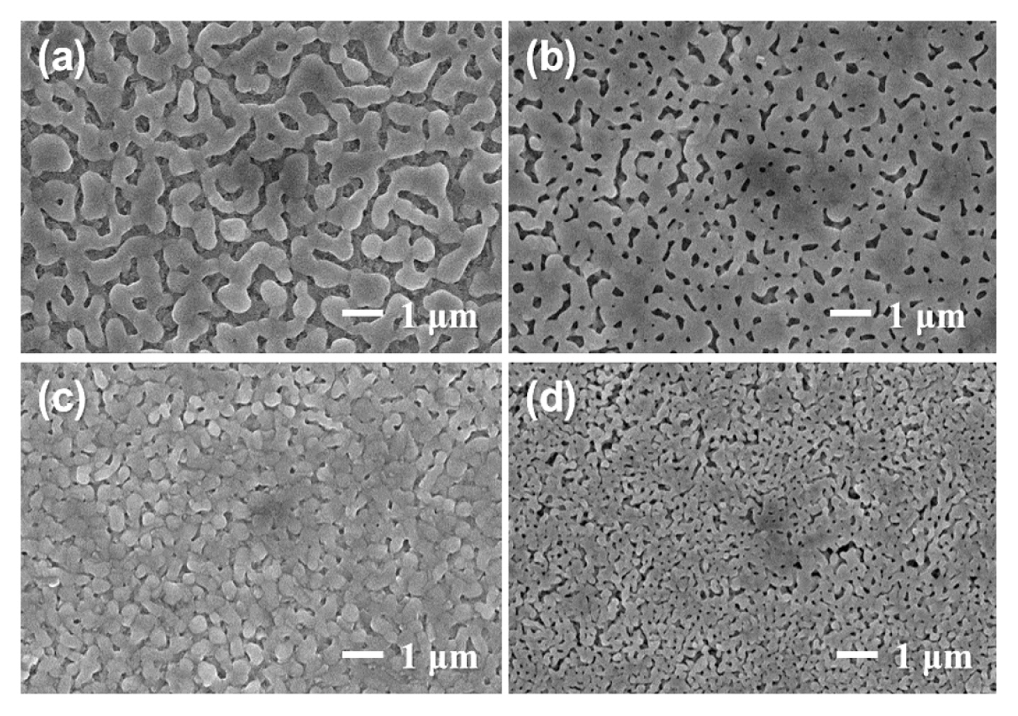
Fig. 1 shows FE-SEM images of the BiVO4, Mo:BiVO4, Al2O3/BiVO4, and Al2O3/Mo:BiVO4 films. All films consisted of differently sized porous areas (briefly denoted as domains) separated from each other by thin grooves. In the case of BiVO4 film (Fig. 1a), within a domain, wormlike pores with a size of several hundreds of nanometers were wholly distributed. Furthermore, the thin groove separating porous domains was completely separated through the entire film (not shown in here) with a thickness of about 200 nm. Meanwhile, the Mo:BiVO4 film (Fig. 1b) exhibited wormlike pores with a size of several tens of nanometers, displaying a relative small amount of pore size ascribed to grain growth of BiVO4 film blocked by the added Mo6+ cations [18]. Above these films, ultra-thin Al2O3 layer was deposited by ALD process. Their images are shown in Fig. 1c and 1d. Al2O3/BiVO4 and Al2O3/Mo:BiVO4 films exhibited overall similar morphologies, but their wormlike nanopores in a domain were steadily reduced mainly due to steady growth of BiVO4 grains with an additional thermal annealing process under 450°C, not contributed from just 2-nm thick Al2O3 layer. Entirely Al2O3 covered nanoporous BiVO4 films were observed.
Crystalline characteristics and optical properties of BiVO4, Mo:BiVO4, Al2O3/BiVO4, and Al2O3/ Mo:BiVO4 films were surveyed using XRD measurement (Fig. 2a) and UV-VIS spectroscopy (Fig. 2b). Dotted vertical lines in Fig. 2a refer to peaks from the FTO substrate. The XRD pattern of the pristine BiVO4 film (Fig. 2a) after calcined at 500°C under air ambient showed well crystallized monoclinic structure corresponding to (013), (004), (024) and (116) planes with lattice parameters of a = 5.195, b = 5.093 and c = 11.704 Å, in excellent accordance with the standard data (JCPDS NO.: 83–1699) [19]. No other peaks for impurity or other binary or ternary compounds were found anywhere, thereby showing the development of a high-quality BiVO4 film. In the case of Mo:BiVO4 film, the position and intensity of all peaks had similar patterns to those of the BiVO4 film probably due to the extremely small amount of molybdate precursor. Furthermore, no modification or change of peaks after Al2O3 coating was found through the entire film, only showing a little bit reduction of peak intensity. In addition, the average crystalline size was calculated using Scherrer’s equation, considering the main peak of (221) plane in all samples. Average crystalline sizes of BiVO4, Mo:BiVO4, Al2O3/BiVO4, and Al2O3/ Mo:BiVO4 films were 19.3 nm, 19.4 nm, 19.3 nm, and 19 nm, respectively, disclosing no significant difference in average crystalline size even after deposition of thin Al2O3 layer.
Fig. 2b shows optical absorbance of BiVO4, Mo:BiVO4, Al2O3/BiVO4, and Al2O3/Mo:BiVO4 films fabricated on FTO substrate. The BiVO4 and Mo:BiVO4 film started to absorb light at the wavelength of 525 nm. Its overall absorbance spectra showed similar tendency. Meanwhile, the ultra-thin Al2O3 coated film showed degraded absorbance, showing a little bit reduction of the absorbance and the shift of onset wavelength toward longer wavelength. The exact direct optical bandgap (Eg) was determined for all samples by extrapolating linear portion of the (αhν)2 vs. hν plot as shown in the inset of Fig. 2b, where α was the absorption coefficient and hν was the incident photon energy [20]. Estimated Eg values of BiVO4, Mo:BiVO4, Al2O3/ BiVO4, and Al2O3/Mo:BiVO4 films were 2.36 eV, 2.34 eV, 2.34 eV, and 2.20 eV respectively. The slightly reduced Eg value was observed in Mo:BiVO4 film after the ultra-thin Al2O3 coating, indicating the formation of sub-bandgap just below the conduction band of Mo:BiVO4 film, resulting in the extension of visible light absorption to wavelength of 560 nm.
To determine electronic characteristics of the BiVO4 film, Mott-Schottky plots were measured in 0.5 M Na2SO4 solution as a function of applied potential. Results are displayed in Fig. 3. The Mott- Schottky plot (M-S plot) was involved in the capacitance (C) of the space charge region as a function of electrode potential under depletion conditions. It was based on the Mott-Schottky relationship of a semiconductor film. Accordingly, these results gave the information on carrier densities through the gradient dV/d(1/C2) of Mott–Schottky plots and flat band potential (Efb) determined by extrapolating C = 0 [21].
where e0 was electronic charge, ɛ was dielectric constant (~ 86) of BiVO4, ɛ0 was permittivity of the vacuum, Nd was donor density, and V was the applied voltage. All BiVO4 films exhibited positive slopes as expected for n-type semiconductor. In particular, ultra-thin Al2O3 coated films showed smaller slope than pristine BiVO4 and Mo:BiVO4 films, manifesting increased carrier densities. Quantitatively calculated electron densities of BiVO4, Mo:BiVO4, Al2O3/ BiVO4, and Al2O3/Mo:BiVO4 were calculated to be 1.52 × 10¹⁷, 3.44 × 10¹⁸, 2.6 × 10¹⁷, and 4.2 × 1018 cm−3, respectively. Here, Mo:BiVO4 film showed approximately one order of magnitude higher donor densities than the pristine BiVO4 film probably due to increased carrier densities induced from Mo doping which could contribute to the improvement of electrical conductivities of Mo:BiVO4 film [22]. In addition, the introduction of ultra-thin Al2O3 layer on the top surface of film improved carrier densities a little bit probably ascribed to the high probability of photo-generated charges surviving against the charge recombination reaction. The extent of high carrier densities was as follows: BiVO4 < Al2O3/BiVO4 < Mo:BiVO4 < Al2O3/Mo:BiVO4. In case of flat-band potential (VFB), BiVO4 and Mo:BiVO4 films showed VFB of 0.18 VRHE and 0.28 VRHE, respectively, whilst VFB of 0.067 VRHE and 0.16 VRHE were obtained for Al2O3/BiVO4 and Al2O3/Mo:BiVO4 films, respectively. A little bit negative shift of VFB was observed in Al2O3/BiVO4 and Mo:BiVO4 films probably due to the high-band gap Al2O3 (Eg ≈ 3.6 eV) layer.
In order to investigate PEC activities of BiVO4, Mo:BiVO4, Al2O3/BiVO4, and Al2O3/Mo:BiVO4 films, linear sweep voltammograms (LSVs) were measured under AM1.5 illumination. Results are presented in Fig. 4a. The dark current of BiVO4, Mo:BiVO4, Al2O3/BiVO4, and Al2O3/Mo:BiVO4 films collected in the potential range between 0.0 and 1.5 VRHE under the dark condition exists in the region of ~10−3 mA/cm2, showing no meaningful current values (not shown here). At first, onset potentials of BiVO4 and Mo:BiVO4 were near 0.33 and 0.19 VRHE, respectively while Al2O3/BiVO4 and Al2O3 / Mo:BiVO4 films exhibited onset potentials of 0.05 and 0.1 VRHE, respectively, displaying a little bit negative shift of onset potential. These results were similar to those evoked from Mott-Schottky plot probably due to surface passivation from the ultra-thin Al2O3 layer. Herein, the photocurrent density (J) of 0.12 mA/cm2 at 1.23 VRHE was achieved for the pristine BiVO4 film. On the other hand, the Mo:BiVO4 film had a quite high J value of 0.86 mA/cm2 at 1.23 VRHE. On the contrary, Al2O3/BiVO4 and Al2O3/Mo:BiVO4 films showed J values of 0.91 mA/cm2 and 1.5 mA/cm2 at 1.23 VRHE, respectively. These results indicated that the ultra-thin Al2O3 layer promoted J values of intrinsic BiVO4 and Mo:BiVO4 films. Furthermore, the Co-Pi cocatalyst was deposited on the top surface of Al2O3/Mo:BiVO4 films, showing the most enhanced J value of 1.85 mA/cm2 at 1.23 VRHE due to favorably hole transfer to the electrolyte under the cascading hole transferring phenomenon.
To determine photoactivities as a function of the illuminated wavelength of BiVO4, Mo:BiVO4, and Al2O3 deposited films, we quantitatively investigated the photoactivity as a function of wavelength of incident light referred to as incident photon-to-current conversion efficiency (IPCE). IPCE measurements were performed for BiVO4, Mo:BiVO4, Al2O3/ BiVO4, and Al2O3/Mo:BiVO4 films using an applied potential of 1.23 VRHE (Fig. 4b). IPCE can be generally expressed by the following equation [23];
where J is the measured photocurrent density at a specific wavelength, λ is the wavelength of incident light, and Jlight is the measured irradiance at a specific wavelength. In comparison with the pristine BiVO4 film, Mo:BiVO4 films exhibited significantly enhanced IPCE over the entire UV and visible light region. Particularly, the onset wavelength to start to give a meaningful photo-response was tremendously shifted from 510 nm to 530 nm, further going to 550 nm (Al2O3/Mo:BiVO4) and 570 nm (Co-Pi/ Al2O3/Mo:BiVO4). These results provide direct evidence showing increased visible light photoresponse of Mo:BiVO4 film by Mo doping thanks to more survived photogenerated charges from the deposition of ultra-thin Al2O3 layer against the charge recombination process. In addition, the Mo:BiVO4 film exhibited IPCE of 15.6% (@486 nm) whereas the BiVO4 film had an IPCE of 5.7% (@486 nm). Al2O3 coated samples exhibited IPCE of 22% (Al2O3/Mo:BiVO4) and 7% (Al2O3/BiVO4) at the same wavelength, indicating that charge transfer/transportation events were very efficient in these Mo-doped and Al2O3-coated samples. Moreover, the Co-Pi deposited Al2O3/ Mo:BiVO4 film showed remarkably red-shifted IPCE curve, containing a shift of λmax toward 500 nm having an IPCE value of 22.5% promoted by the more contribution of visible light-induced charges. Therefore, both Mo-doping and Al2O3 coating contributed to the improvement of PEC performance mainly coming from the more charges photogenerated from visible light.
To definitely examine the interfacial issues, electrolyte interface capacitance as a function of the applied potential under dark condition was measured using the electrochemical capacitive current scan method [24]. Results are presented in Fig. 5a. Both BiVO4 and Mo:BiVO4 films exhibit a peak centered at about +0.75 VRHE previously characterized as evidence for a surface state by Bard et al [25]. However, these peaks disappeared after the deposition of ultra-thin Al2O3 layer, proving the role of surface passivation. Overall, capacitance values of BiVO4 and Mo:BiVO4 films were significantly decreased, manifesting that the insulating Al2O3 layer as an outermost layer could dramatically reduce charge storage in the BiVO4 film, enabling fast charge transfer or blocking nearby films or electrolyte.
To investigate minutely the interfacial working condition according to Mo-doping and Al2O3 coating in the BiVO4 film, EIS measurements under dark condition were conducted. Results are shown in Fig. 5b. Fig. 5b compares the Nyquist plots for BiVO4, Mo:BiVO4 and Al2O3 coated films including the fitting data using the equivalent circuit in which Rs indicates the series resistance which includes FTO substrate, the resistance associated with the ionic conductivity in the electrolyte, and the external contact resistance. Rct is related to the semiconductor/ electrolyte charge transfer resistance at the low-frequency arc [26]. In our system, similar Rs of about 98 (± 4) Ω was achieved in the similar working condition. Rct of the intrinsic BiVO4 film was about 104 value, existing a quite high value. The Mo:BiVO4 film exhibited abruptly reduced Rct of about 17000 Ω, further showing decreased Rct values after Al2O3 coating. This may be explained by the beneficial charge transfer at the interfacial region in the Mo:BiVO4 film that was further improved by the introduction of ultra-thin Al2O3 layer to the scale of 103. This dedicates that the Al2O3 layer can promote photogenerated hole transfer from the electrode to electrolyte as well as passivate the surface defect or traps sites, leading to more survived photogenerated charges to enhance PEC performance. To clearly confirm the extent of charge recombination, the open-circuit photovoltage was measured, presented in Fig. 6. The photovoltage-time (V-t) profile of BiVO4, Mo:BiVO4, Al2O3/BiVO4, and Al2O3/ Mo:BiVO4 films and the decay lifetimes of each V-t spectra by fitting to a biexponential function with two-time constants were calculated [27].
where τm is the harmonic mean of the lifetime, and the total half-life is log (2 × τm). The total half-life of BiVO4, Mo:BiVO4, Al2O3/BiVO4, and Al2O3/ Mo:BiVO4 films was estimated to be 2.58s, 1.10s, 1.31 and 0.89s respectively. This result indicates that the Al2O3/BiVO4 film shows shorter decay lifetime than that of BiVO4 and Mo:BiVO4 films. This was resulted from the modification of BiVO4 to form the ultra-thin Al2O3 layer as well as the Mo doping, which favored good electron transporting paths by the Mo doping and suppressed recombination of photoinduced carriers from the ultra-thin Al2O3 layer.
It is well known that the ultra-thin Al2O3 layer can block photocorrision of BiVO4 layer under illumination. To confirm the photostability of Al2O3 coated films in our system, changes of photocurrent densities as a function of time were detected for BiVO4, Mo:BiVO4, Al2O3/BiVO4, and Al2O3/Mo:BiVO4 films at a constant potential of 1.23 VRHE for 30 min. Results are displayed in Fig. 7. Both pristine and Mo:BiVO4 films exhibited steadily decrease of J value as time went by. Reversely, ultra-thin Al2O3 coated films maintained almost the same J value compared to their initial J values. These results indicate that the ultra-thin Al2O3 layer can also suppress the corrosion of photoelectrode under illumination in our system.
In summary, uniform coating of thin Al2O3 layer having a thickness of approximately 2 nm on BiVO4 and Mo:BiVO4 films was successfully developed. Based on these well-made Al2O3/BiVO4 and Al2O3/ Mo:BiVO4 films, the PEC performance of Al2O3/ Mo:BiVO4 film was found to be the highest, showing photocurrent density of 1.5 mA/cm2 at 1.23 VRHE attributable to the improved electronic conductivity deduced from Mo doping and surface passivation on the defect or trap sites from ultra-thin Al2O3 layer as well as to favorably transfer of photogenerated holes to electrolyte. In particular, the interfacial resistance (Rct) was sharply reduced in the Mo-doped and Al2O3 coated BiVO4 film. This demonstrates that deposition of ultra-thin Al2O3 layer on the top of BiVO4 film can grant a favorable environment for charge transport/ transfer in the film irrelevant to the presence or absence of doping.
BiVO4 and Mo:BiVO4 films were prepared by the facile sol-gel assisted spin-coating method. Ultra-thin Al2O3 layer with a thickness of 2 nm was uniformly coated by the ALD process. All films were composed of differently sized porous area, separated from each other by thin grooves. Above these films, ultra-thin Al2O3 layer steadily reduced wormlike nanopores, showing uniformly coated nanoporous layer through the entire surface of BiVO4 film. Overall, Al2O3/ Mo:BiVO4 film exhibited the highest photocurrent density (1.5 mA/cm2 at 1.23 VRHE), followed by Al2O3/BiVO4 film (0.91 mA/cm2), Mo:BiVO4 film (0.86 mA/cm2), and BiVO4 film (0.12 mA/cm2). This is from the enhanced electronic conductivity of Mo doping in the BiVO4 film and coating of ultra-thin Al2O3 layer to retard the charge recombination reaction as well as the beneficial hole transfer to the electrolyte. Herein, the Co-Pi layer as a cocatalyst was deposited on the Al2O3/Mo:BiVO4 film, displaying a photocurrent density of 1.85 mA/cm2 at 1.23 VRHE due to low interfacial resistance to promote favorable hole transfer to the electrolyte. The IPCE curve also showed the highest value of about 22.5% at 500 nm for Co-Pi/Al2O3/Mo:BiVO4, followed by 22% for Al2O3/Mo:BiVO4, 7% for Al2O3/BiVO4, and 5.7 % for BiVO4 at wavelength of 486 nm. From Mott-Schottky plot, Al2O3/Mo:BiVO4 film showed the highest electronic conductivity probably due to Mo doping and surface passivation of ultra-thin Al2O3 layer at the defect or trap sites, leading to reduced electron-hole recombination. These results were similar to the trend of interfacial resistance (Rct) in the Nyquist plot obtained from EIS measurement, showing that Mo doping and the coating of Al2O3 layer together induced the abrupt decrease of Rct, overall influencing the advancement of PEC activity. Taken together, these results indicate that coating or deposition of proper materials in the thin film can modify or alternate thin film to enhance its PEC performance.
Acknowledgement
This research was supported by Basic Science Research Capacity Enhancement projuect through Korea Basic Science Institute (National research Facilities and Equipment Center) grant furded by rhe Ministry of Education (2019RIA6C1010024) and the samples were treated by using ALD at Energy Convergence Core Facility in Chomma National University. This work was also supported by a grant (2018R1A6A1A03024334) of the Priority Research Centers Program through the National Research Foundation of Korea (NRF) funded by the Ministry of Education, Science and Technology.
Fig. 2
(a) XRD patterns and (b) absorbance spectra of BiVO4, Mo:BiVO4, Al2O3/BiVO4, and Al2O3/Mo:BiVO4 films.
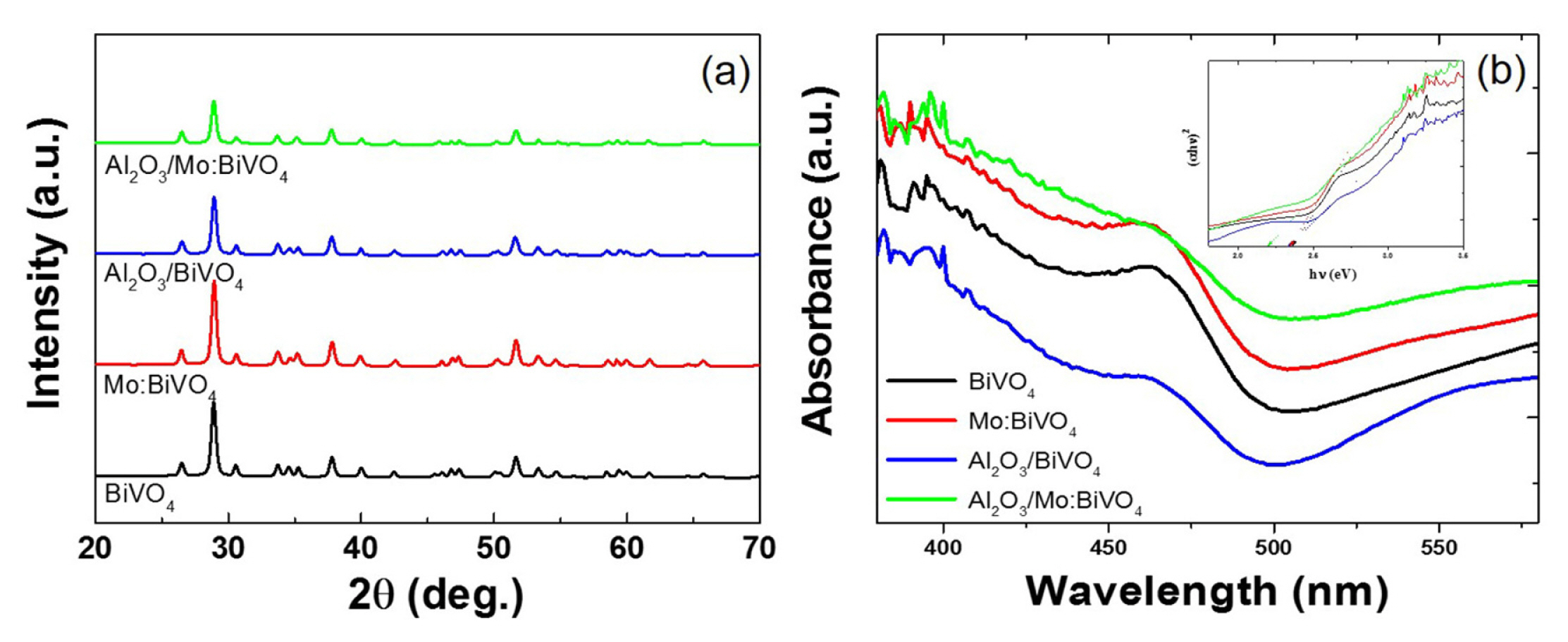
Fig. 3
Mott-Schottky plots of BiVO4, Mo:BiVO4, Al2O3/ BiVO4, and Al2O3/Mo:BiVO4 films measured in 0.5 M Na2SO4 solution under dark condition.
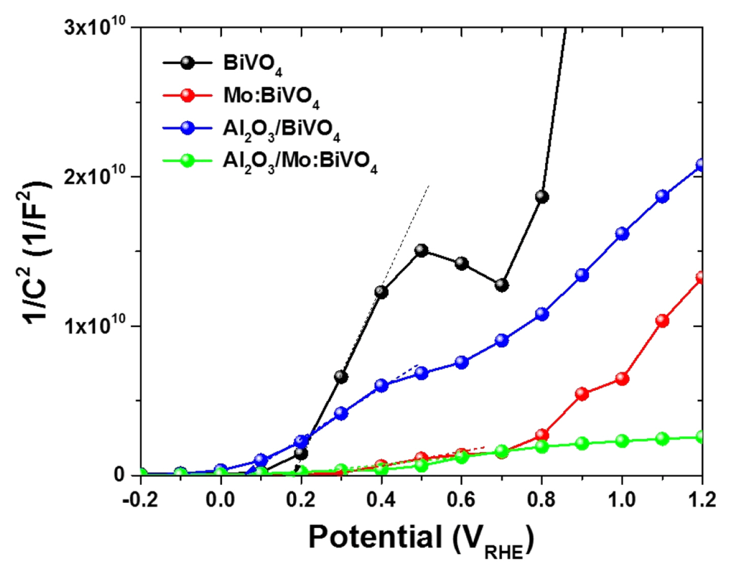
Fig. 4
(a) J-V curves of BiVO4, Mo:BiVO4, Al2O3/BiVO4, Al2O3/Mo:BiVO4, and Co-Pi/ Al2O3/Mo:BiVO4 films under solar light (100 mW/cm2 with AM 1.5) in 0.5 M Na2SO4 solution and (b) IPCE spectra of BiVO4, Mo:BiVO4, Al2O3/ BiVO4, Al2O3/Mo:BiVO4, and Co-Pi/ Al2O3/Mo:BiVO4 films measured with applied potential of 1.23 VRHE in 0.5 M Na2SO4 solution.

Fig. 5
(a) Capacitance value as a function of the applied potential for BiVO4, Mo:BiVO4, Al2O3/BiVO4, and Al2O3/ Mo:BiVO4 films under dark condition and (b) Nyquist plots of BiVO4, Mo:BiVO4, Al2O3/BiVO4, and Al2O3/Mo:BiVO4 film containing fitted data using the suggested equivalent circuit in the inset of (b).
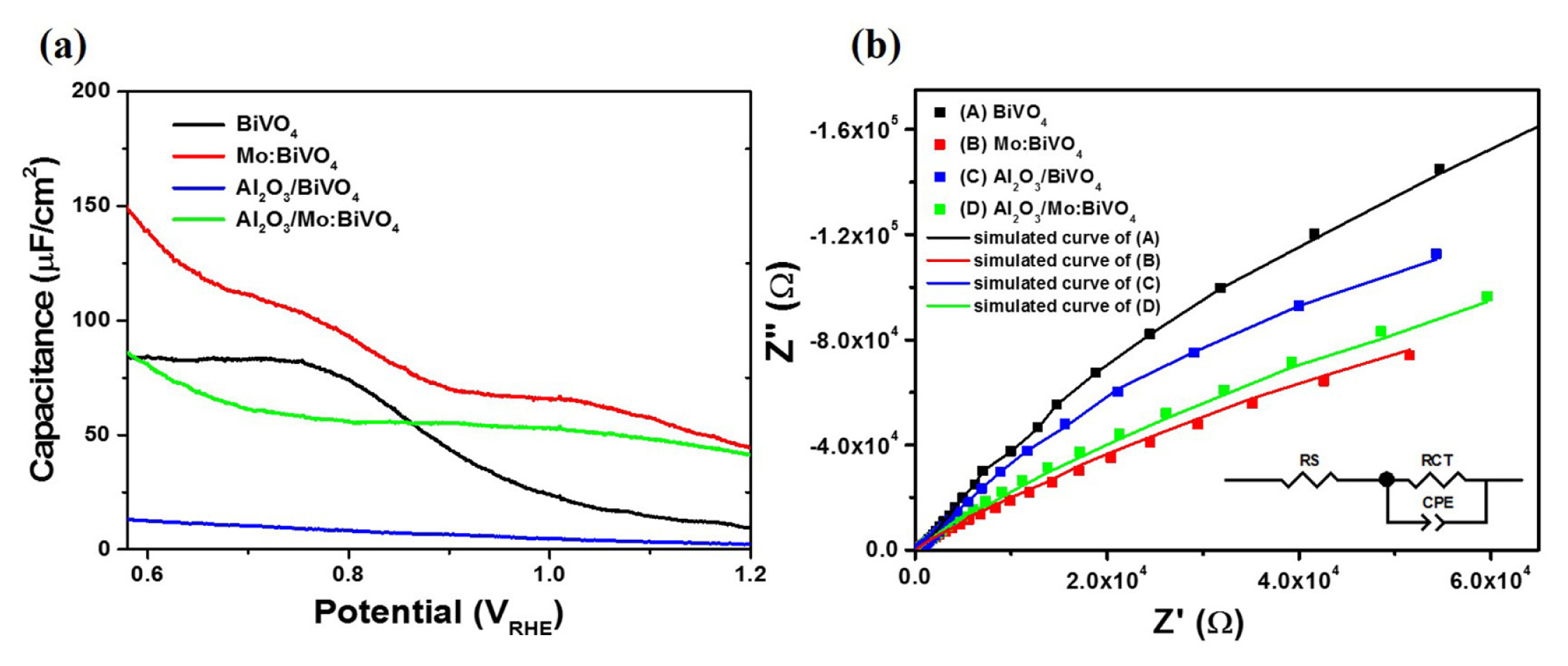
Fig. 6
Open-circuit voltage decay curve of BiVO4, Mo:BiVO4, Al2O3/BiVO4, and Al2O3/Mo:BiVO4 films as a function of time after turning off the light.
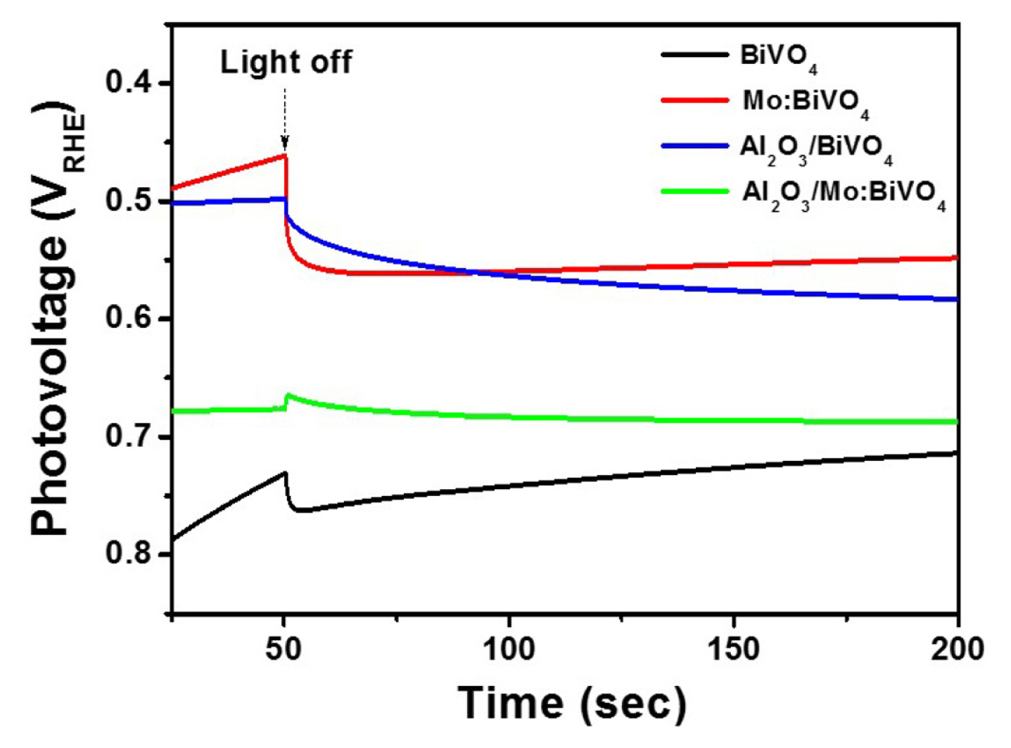
Fig. 7
Photocurrent density as a function of time for BiVO4, Mo:BiVO4, Al2O3/BiVO4, and Al2O3/Mo:BiVO4 films in 0.5 M Na2SO4 solution.
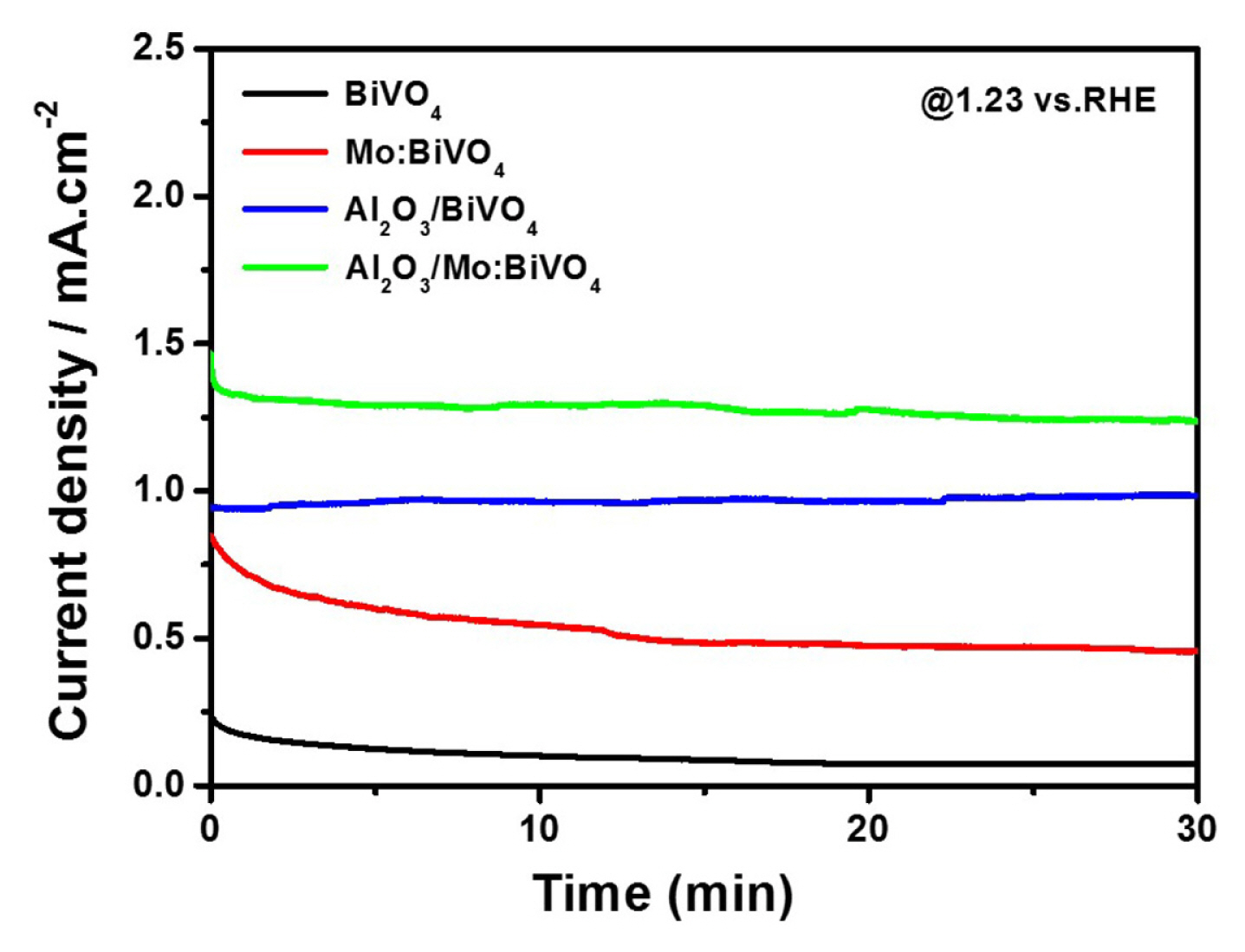
Table 1
Flat band potential (VFB) and donor densities (Nd) of BiVO4, Mo:BiVO4, Al2O3/BiVO4, and Al2O3/Mo:BiVO4 films.
| Samples | Flatband potential (VFB, V) | Donor density (Nd, cm−3) |
|---|---|---|
| BiVO4 | 0.19 | 1.52×10¹⁷ |
| Mo:BiVO4 | 0.31 | 3.44×10¹⁸ |
| Al2O3/BiVO4 | 0.1 | 2.6×10¹⁷ |
| Al2O3/Mo:BiVO4 | 0.31 | 4.2×10¹⁸ |
Table 2
Quantitative value of ohmic resistance (Rs) and charge transfer resistance (Rct) of BiVO4, Mo:BiVO4, Al2O3/BiVO4, and Al2O3/Mo:BiVO4 films fitted by using the suggested equivalent electrical circuit.
| Samples | Rs (Ω) | Rct (Ω) |
|---|---|---|
| BiVO4 | 102 | 72432 |
| Mo:BiVO4 | 96 | 17012 |
| Al2O3/BiVO4 | 94 | 4441 |
| Al2O3/Mo:BiVO4 | 96 | 2904 |
References
[1] MG. Walter, EL. Warren, JR. McKone, SW. Boettcher, Q. Mi, EA. Santori and NS. Lewis, Chem Rev, 2010, 110(11), 6446–6473.

[4] A. Malathi, J. Madhavan, M. Ashokkumar and P. Arunachalam, Appl Catal A General, 2018, 555, 47–74.

[6] FF. Abdi, L. Han, AHM. Smets, M. Zeman, B. Dam and R. Van De Krol, Nat Commun, 2013, 4, 2195.
[8] G. Yun, M. Arunachalam, H-S. Kim, K-S. Ahn and SH. Kang, J Phys Chem C, 2016, 120(11), 5906–5915.

[12] K. Sun, FH. Saadi, MF. Lichterman, WG. Hale, ST. Omelchenko and J-H. He, Proc Natl Acad Sci, 2015, 112(12), 3612–3617.

[15] Y. Kuang, Q. Jia, G. Ma, T. Hisatomi, T. Minegishi, H. Nishiyarna, M. Nakabayashi, T. Yamada and A. Kudo, Nat Energy, 2017, 2(1), 16191.
[17] SK. Pilli, R. Janarthanan, TG. Deutsch, TE. Furtak, LD. Brown, JA. Turner and AM. Herring, Phys Chem Chem Phys, 2013, 15(35), 14723–14728.

[18] M. Rohloff, B. Anke, S. Zhang, U. Gernert, C. Scheu, M. Lerch and A. Fischer, Sustain Energy Fuels, 2017, 1(8), 1830–1846.

[21] HE. Cho, G. Yun, M. Arunachalam, K-S. Ahn and SH. Kang, J Electrochem Sci Tech, 2010, 9, 282–291.


[23] G. Yun, GY. Song, VH. VQuy, J. Heo, H. Lee, K-S. Ahn and SH. Kang, ACS Appl Mater Interfaces, 2015, 7(36), 20292–303.


