


1. Introduction
With tremendous growth in the worldŌĆÖs population, the energy demand also increases proportionately [1]. The energy demand in 2025 is expected to be twice that of todayŌĆÖs energy demand, which is approximately 15 TW [1]. Though majority of this demand is fulfilled by the fossil fuels, they are not promising energy sources forever and they also pose pollution problems [2]. The reliable alternative to fulfill this energy requirement is solar energy [2]. Majority of the solar cells used today are single crystal silicon or polycrystalline silicon type which are indirect bandgap materials [3]. Apart from being expensive, silicon suffers from the disadvantage of having low absorption coefficient. This requires a very thick absorber layer for silicon based solar cells for effective absorption [3]. To overcome these constraints, the focus has turned towards thin film solar technologies using direct bandgap materials as absorber materials [4]. Commonly used absorber materials for thin film photovoltaic technologies are copper indium gallium diselenide (CIGS), copper indium diselenide (CIS) and cadmium telluride (CdTe) [5]. With limited availability of indium (In) and selenium (Se) along with toxicity issues arising out from the cadmium usage, the search for suitable absorber material for thin film technology is still going on [5]. Studies in search of an inexpensive and environmental friendly absorber material with direct band gap have identified Cu2ZnSnS4 (CZTS) as the promising candidate which is a quaternary semiconductor with high absorption coefficient of 104 cmŌłÆ1 [6]. The highest reported photoconversion efficiency for CZTS based solar cells is 12.6% according to the studies in 2014 [6]. Like other photovoltaic materials, CZTS thin films can also be prepared by various physical and chemical routes [1]. High energy techniques such as atom beam sputtering, radio frequency (RF) magnetron sputtering, thermal evaporation, pulsed laser deposition, spray pyrolysis have been employed to form CZTS thin films [1]. On the other hand, low energy techniques such as sol-gel spin coating, chemical spray pyrolysis, successive ionic layer adsorption and reaction, chemical bath deposition, electrochemical deposition have also been employed to form CZTS thin films [7]. Among these low energy routes, electrochemical deposition of CZTS is the most promising technology [3]. The first study on electrochemical deposition of CZTS reported multistep electrochemical deposition of CZT followed by sulfurization during annealing [8]. Electroplating was also studied to deposit CZT followed by high temperature annealing in sulfur environment [9]. Multistep electrodeposition with high temperature annealing with different electrolytes has been studied extensively [9-12]. In a study on multistep electrodeposition of CZTS, a cyanide-free electrolytic bath consisting of the Cu, Sn and Zn precursors was used as electrolyte for Cu, Zn and Sn co-electrodeposition on Mo coated glass slides. After coating of Cu, Zn and Sn on the Mo substrate, sulfur was added to the deposits by sulfurization in Ar/H2S environment with 5 vol% H2S. The CZTS film thus formed was used to fabricate the solar cell which showed an efficiency of 3.4% [9]. In another study, multistep underpotential electrodeposition called as electrochemical atomic layer epitaxy (ECALE) was used to deposit CZTS [11]. Co-electrodeposition where two or more metals are deposited in a single step is preferred to multistep electrode-position processes. Co-electrodeposition processes generally involve selection of precursors which are very close to each other in electromotive force (e.m.f) series or use of complexing agent which reduces the differences in the deposition potential [13]. Co-electrodeposition of Cu, Zn and Sn followed by sulfurization during annealing has also been reported [14,15]. One critical issue with sulfur incorporation during annealing is the volumetric expansion of the CZTS layer which has negative impact on the performance [16-18]. To overcome this issue, single step electrodeposition incorporating sulfur during electrodeposition has been proposed [16,17,19]. The major concern with single step electrodeposition of CZTS is the widely spaced reduction potentials of Cu, Zn, Sn and S [20]. The standard reduction potential of Cu, Zn and Sn in uncomplexed state are +0.34 V, ŌłÆ0.76 V and ŌłÆ0.14 V respectively [8,21]. With significant difference in the standard reduction potentials of Cu, Zn and Sn, the role of complexing agents in shifting the reduction potentials to achieve CZTS deposits of desired stoichiometry in a single step is inevitable [21]. In many co-electrodeposition processes involving multiple elements, complexing agents are useful to bring the reduction potentials of the elements closer as already mentioned [20,22]. Trisodium citrate, tartaric acid and sorbitol have been found to be suitable complexing agents for single step electrodeposition of CZTS on metal and on transparent conducting oxide substrates [15-17,24,25]. In a study on single step electrodeposition of CZTS on ITO coated substrate, tri-sodium citrate and tartaric acid were used as the complexing agents. The deposition potential used for cathodic electrodeposition process was ŌłÆ1.05 V vs. SCE. The deposits were then annealed in Ar environment at 550┬░C for 1 h. The CZTS deposits were found to have desired stoichiometry of 2:1:1:4 for Cu:Zn:Sn:S [17]. Sodium thiocyanate is one of the most commonly used complexing agents in many commercial electroplating formulations. Use of sodium thiocyanate for CGS electrodeposition has been reported [21]. Recently, our group reported the use of sodium thiocyanate as the complexing agent for single step electrodeposition of CZTS with an electrolyte consisting of 20 mM Cu, Zn, Sn and S and 2.5 M sodium thiocyanate [22]. The study showed that the quality of the deposits was influenced significantly by the pH of the electrolyte. However, detailed investigation of the behavior of individual precursor in the system and characterization of the obtained deposits were not made.
This work discusses in detail single step electrochemical deposition of CZTS on transparent indium tin oxide (ITO) substrate using sodium thiocyanate as the complexing agent. The work also discusses the effect of pH of the electrolyte used for the deposition on the stoichiometry of the CZTS deposits formed. The deposits formed were characterized using X-ray diffraction (XRD) for crystalline nature, UV-vis spectroscopy (UV-vis) for optical properties, scanning electron microscopy (SEM) and transmission electron microscopy (TEM) for morphology, field - emission gun scanning electron microscopy (FEG-SEM) for thickness of the deposit, energy dispersive X-ray diffraction (EDX) for elemental composition. The resistance of the deposits was studied by IV-characterization technique. The behavior of the individual species in the system was investigated using electrochemical impedance spectroscopy (EIS) studies.
2. Material and Methods
2.1 Material
Indium tin oxide (ITO) coated glass slide from Sigma-Aldrich was used as the substrate. The electrochemical deposition of CZTS was performed under potentiostatic mode. Analytical grades of copper sulfate pentahydrate (CuSO4.5H2O), zinc sulfate heptahydrate (ZnSO4.7H2O), tin chloride (SnCl2) and sodium thiosulfate (Na2S2O3) were used as Cu, Zn, Sn and S precursors respectively. Sodium thiocyanate was used as the complexing agent. Deionized water bubbled with nitrogen was used to prepare the electrolyte. The electrolytic bath used for the electrode-position contained 20 mM of Cu, Sn, and S precursor each and 50 mM of Zn precursor. The concentration of sodium thiocyanate was maintained at 2 M. The pH of the electrolyte was adjusted using either KOH or HNO3 solution.
2.2 Experimental
The electrochemical deposition studies were carried out in an electrochemical workstation (CHI 660E, CH instruments, USA). A three electrode cell configuration was used for the deposition experiments. Working electrode was formed from ITO glass slide of 10 mm ├Ś 10 mm ├Ś 1.1 mm dimension, Ag/AgCl was used as the reference electrode while platinum wire was used as the counter electrode. The suitable deposition potential for the potentiostatic deposition runs was found out from cyclic voltammetry (CV) runs of the electrolyte containing all the precursors with the complexing agent. Cyclic voltammetry was also performed for the electrolytes containing single precursor without and with the complexing agent. The CV runs were performed with a scan rate of 0.05 VsŌłÆ1. The deposition was done under potentiostatic mode for 20 min. The deposits, thus obtained, were washed with deionized water and dried with nitrogen. The deposits were also annealed at 600┬░C in inert environment. The electrochemical impedance spectroscopy was conducted for the individual precursors with 2 M complexing agent at pH 2.5. The deposition potential corresponding to pH 2.5 was used to perform the EIS runs. The EIS runs were conducted for a frequency range from 105 Hz to 1 Hz with potential amplitude of 10 mV rms was used. The results of the EIS runs were analyzed using Zsimpwin software. The morphology of the deposits and the elemental composition were done using SEM (Zeiss Evo-Model EVO 18) and EDX (INCA 250 EDS with X-MAX 20mm Detector) respectively. FEG-SEM (JEOL, JSM-7600F) was used for analyzing the thickness of the CZTS deposition. TEM (Philips, CM 200) was used for the morphology analysis. The UV-visible spectroscopy was performed by dispersing the CZTS particles from the non-annealed deposits in deionized water. The optical properties of the deposits were characterized using the absorption spectra of the samples generated in UV-vis spectrophotometer (Shimadzu, UV-1800). Crystalline nature of the deposits was studied using X-ray diffraction unit (PANalytical 3 kW XŌĆÖpert). I-V characterization studies were done using electrochemical workstation (CHI 660E, CH instruments, USA).
3. Results and Discussion
3.1 Cyclic voltammetry
Fig. 1 shows the cyclic voltammetry runs for the individual precursors, 20 mM Cu, 50 mM Zn, 20 mM Sn and 20 mM S without and with 2 M sodium thiocyanate at pH 2.5. In this work, sodium thiocyanate acts as complexing agent. A complexing agent is believed to change the reduction potential by forming complexes with the ions available in the solution. By formation of the complex, they improve the throwing power of the electrolytic bath [26]. Similarly, pH of the electrolyte significantly affects the stability of the complex, causing shift in the equilibrium between various types of ions in the electrolytic bath resulting in a change in the deposition potential and the deposition rate [27]. In Fig. 1, the solid lines represent the CV spectrum of the precursors with 2 M complexing agent while the dotted lines represent the CV results for the precursors without complexing agent. The CV plot for copper precursor without complexing agent shows well defined peak at ŌłÆ0.32 V and ŌłÆ0.93 V which corresponds to the reduction of Cu2+ to Cu+ and reduction of Cu+ to metallic Cu0 respectively [28]. In the presence of complexing agent, a prominent peak appears at ŌłÆ0.91 V due to the complex formation. The area of the peaks decreased significantly when compared to the uncomplexed one, which could be due to the complexing action of thiocyanate ions. A shift in the cathodic peak potential combined with decrease in the peak current density with the addition of complexing agent is reported to be an indication of better complexing action [29]. Similarly, oxidation process is enhanced which is seen by a well defined peak in the anodic sweep which is not present in the uncomplexed copper system. This clearly indicated that the SCNŌłÆ has better complexing ability with copper precursor [29,30]. The cyclic voltammogram for uncomplexed Zn in Fig. 1 shows a cathodic peak at ŌłÆ1.2 V corresponding to the reduction of Zn2+ whereas with the addition of complexing agent two cathodic peaks appear, one at ŌłÆ1.1 V which has a peak area lower than the uncomplexed system and a major peak at ŌłÆ1.3 V indicating the presence of more than one form of Zn2+ complex in the electrolyte [31,32]. From Fig. 1, it is seen that the addition of complexing agent causes negative shift of the reduction potential by 205 mV in the case of Sn precursor. The cathodic peak potential corresponding to Sn2+ is ŌłÆ0.8 V without complexing agent which decreases to ŌłÆ1.005 V with complexing agent. The current density also showed a significant decrease with complexing agent corresponding to better complexing action.
The cyclic voltammograms for sodium thiosulphate without complexing agent shown in Fig. 1 presents two cathodic peaks, a smaller peak at ŌłÆ0.95 V which correspond to partial decomposition of S2O32ŌłÆ to S and SO32ŌłÆ through electrochemical reaction given in equation 1 in the acidic medium and a more negative well defined peak at ŌłÆ1.27 V which could be attributed to the equations 2 and 3 [33].
Fig.┬Ā1.
Cyclic voltammograms for the individual precursors with and without 2M sodium thiocyanate at pH 2.5.
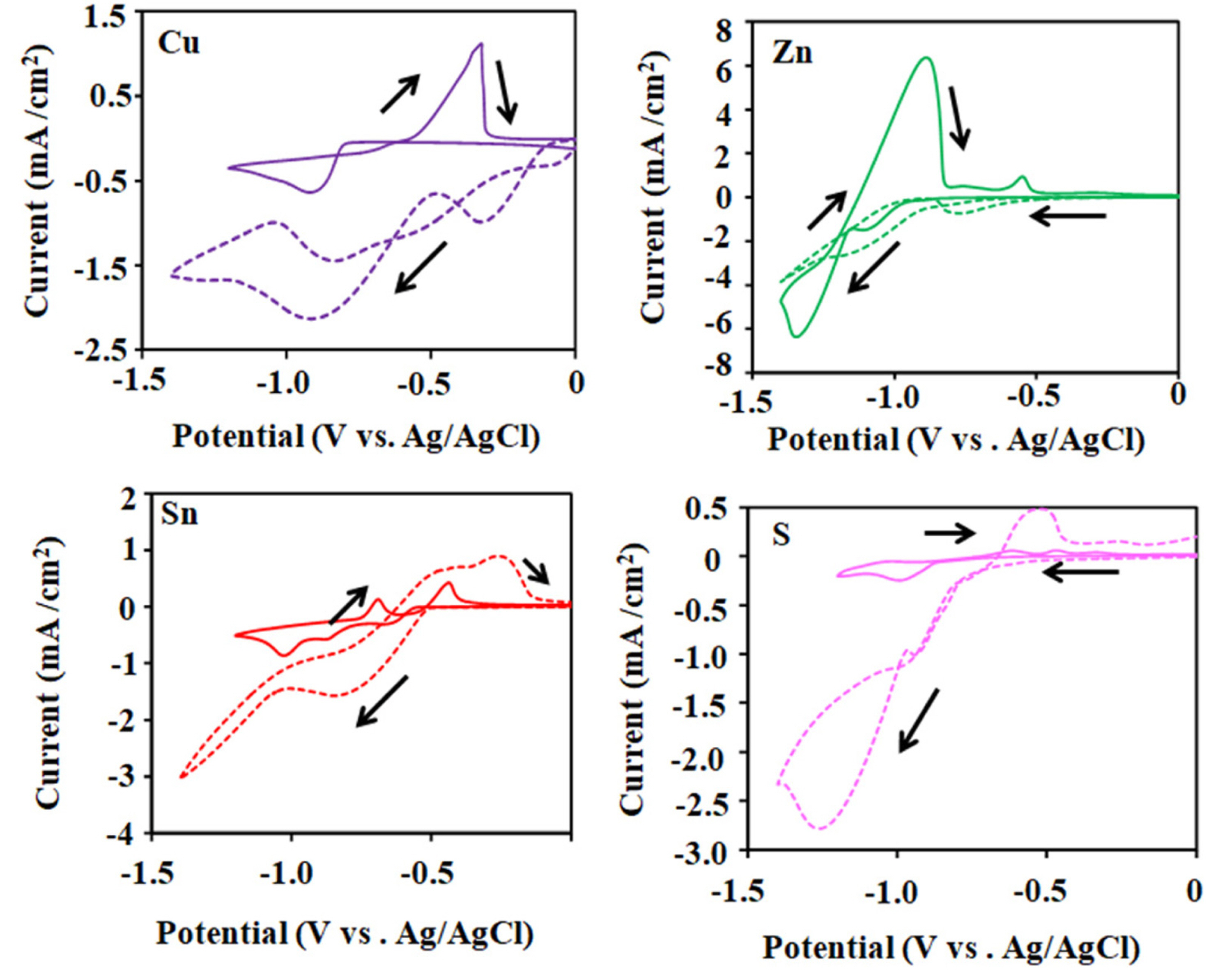


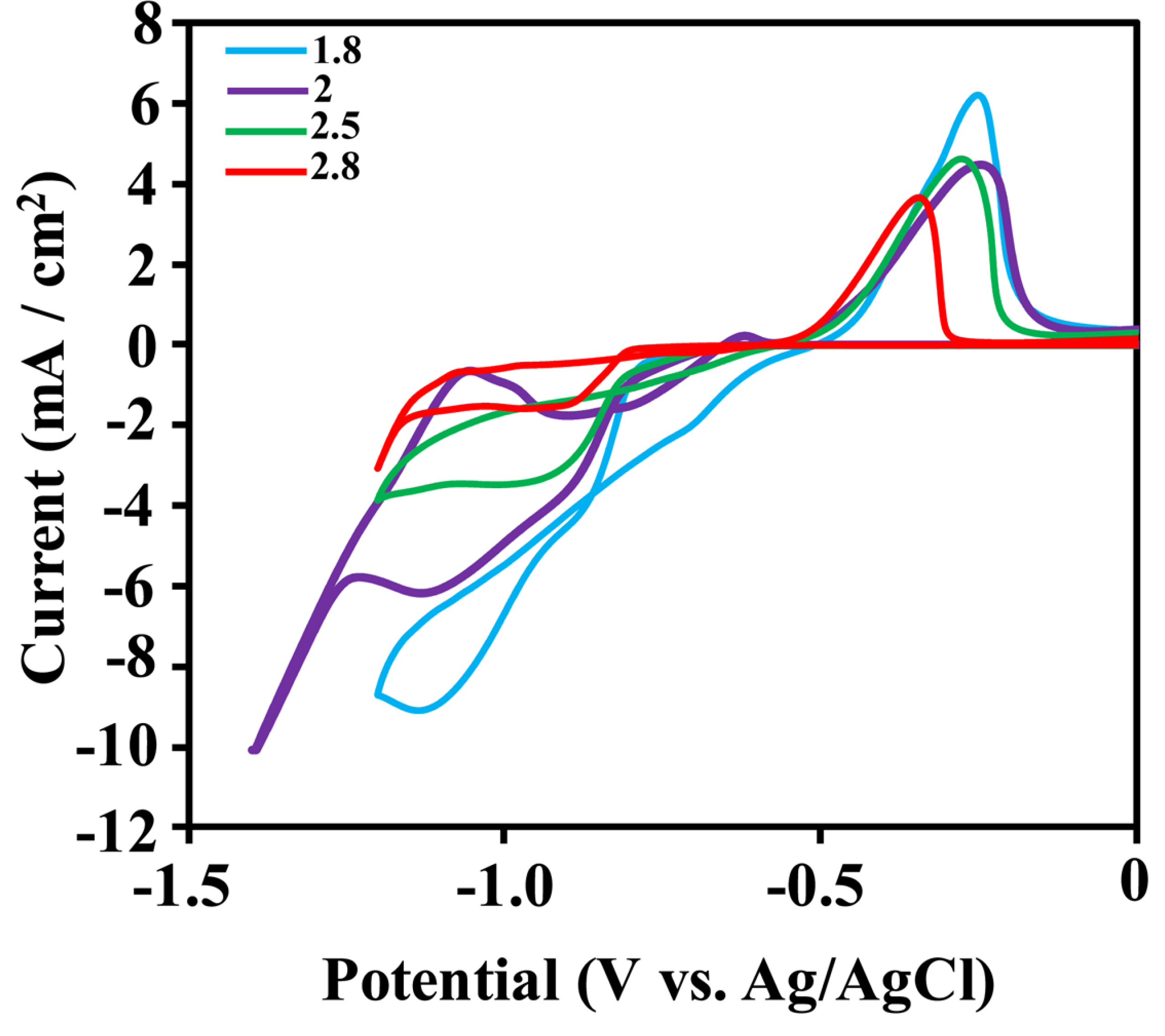
With the addition of thiocyanate, though any complex formation is not anticipated, the peak presents a positive shift and occurs at ŌłÆ1.13V thus decreasing the reduction potential. Such a positive shift in the reduction potential has been observed in the case of cyano compounds on protonation [34]. Based on the observations, addition of thiocyanate thus helps in decreasing the deposition potential window between Cu, Zn, Sn and S and helps in co-deposition. The addition of complexing agents was found to cause shift in reduction potentials due to complex formation with one or many of the ions available in the system [21-24]. The present observation with thiocyanate can also be credited to the varying degree of complexing action of the same with Cu, Zn and Sn ions available in the electrolyte. Fig. 2 shows the CV patterns for the electrolyte which consists of all the four precursors with sodium thiocyanate at pH 1.8, 2, 2.5 and 2.8. The cathodic peak potential for the electrolytes are ŌłÆ1.139 V for pH 1.8, ŌłÆ1.126 V for pH 2, ŌłÆ0.945 V for pH 2.5 and ŌłÆ0.92 V for pH 2.8. The cathodic peak current value is the highest for the electrolytic bath at pH 1.8 which could be due to the increased concentration of H+ ions and decreased diffusion resistance enabling higher deposition rate [35]. Change in the reduction potential value with change in pH could be attributed to the involvement of proton during electron transfer reaction [36].
3.2 X-ray diffraction
Fig. 3 shows the XRD spectra of the CZTS deposits formed at different pH after annealing. The XRD pattern shows that the samples are polycrystalline in nature [37]. It is observed from Fig. 3 that the intensity of some of the peak changes with pH. Similarly, disappearance or appearance of few peaks is also observed. The peaks corresponding to (110), (101), (112) of kesterite phase and the peaks corresponding to (102) of wurtzite phase present a change in the intensity with pH of the electrolytic solution. Similarly, at pH 2.8 there is appearance of new peak at 53.4┬░ corresponding to (130) plane of kesterite phase [38]. Such changes occurring in the peak intensities, appearance and disappearance of peaks can be attributed to structural modifications due to the preferred orientation grain growth, changes in the degree of crystallinity or the variations in the thickness of the deposits obtained at different pH [37,39]. Analysis of the peak positions show the presence of kesterite and wurtzite phase CZTS [40,41]. The peaks at 18┬░, 23┬░, 34┬░, 57┬░, 59┬░, and 69┬░ are attributed to the kesterite phase of CZTS from Joint Committee on Powder Diffraction Standards (JCPDS: 26-0575), and Inorganic Crystal Structure Database (ICSD) #171983) and matches well with the previously reported works [40-43]. Due to the similarities in the atomic arrangements of the two crystal forms, kesterite and wurtzite, some of the diffraction peaks for these two structures are at same positions [40]. The diffraction peaks at 28┬║, 47┬║, and 56┬║ can thus be attributed to (112), (220) and (312) planes of kesterite phase or (002), (110) and (112) planes of wurtzite phase of CZTS [40,41]. The XRD spectrum also shows the presence of many secondary phases like SnS, SnS2, Cu4SnS4, Cu2Sn3S7 [44]. The crystallite size of the deposits can be calculated using the Debye- ScherrerŌĆÖs formula given by Eq. 4 [45].


In Eq. 4, ╬╗ is the incident X-ray wavelength (1.54 ├ģ), ╬▓ is the broadening of diffraction line, full width at half maximum (FWHM) in radians, ╬Ė is the diffraction angle of the prominent peak [18,45,46]. The average crystallite size of the deposits considering all the peaks corresponding to the different crystallite phases for the samples deposited at pH 1.8, 2, 2.5 and 2.8 were found to be 30 nm, 23 nm, 28 nm and 30 nm respectively. The crystallite size presents a monotonic trend. Such behavior where a particular parameter cannot be accounted for the variation in crystallite size has been reported already [47]. In a study by Aslan et al. the crystallite size of the CZTS presents continuously increasing trend, however the thickness of the deposits did not present a regular increasing or decreasing trend. The sulfur content of the deposits however, were found to increase with pH. Thus, the crystallite size of the CZTS deposits was found to be influenced by the sulfur content and the thickness of the deposits [47]. A similar behavior has been observed for the crystallite size in the present study which could be attributed to the thickness and the sulfur content, a part of which may evaporate during annealing affecting the morphology of the deposits.
3.3 UV vis spectroscopy
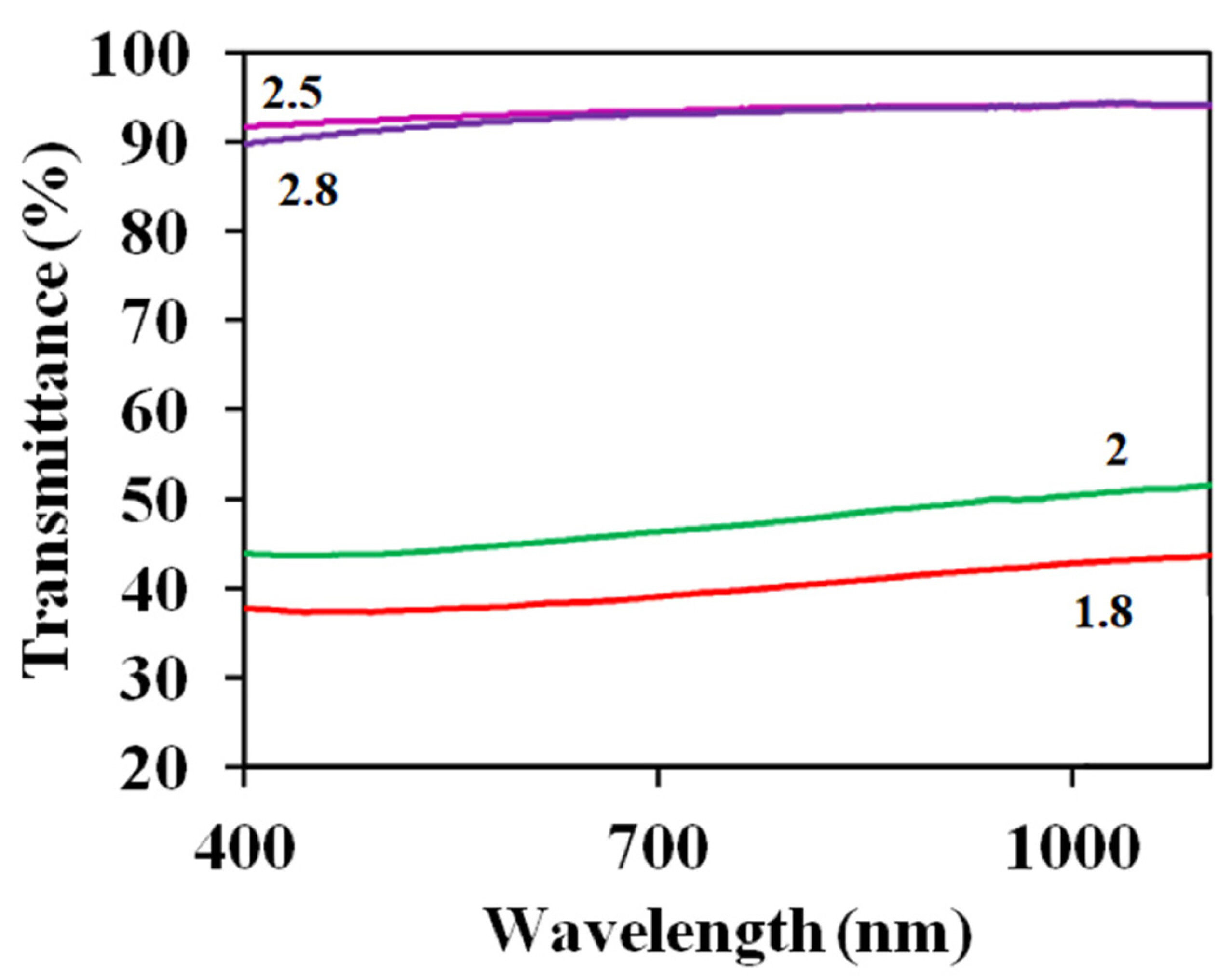
The transmittance spectra of the annealed CZTS samples deposited at different pH is shown in Fig. 4. It is seen that the transmittance values of the samples change significantly with the pH of the electrolyte. The transmittance values for the samples synthesized at pH 1.8 and 2, are less than 50%, whereas, the samples deposited at pH 2.5 and 2.8 show higher transmittance values. In a study on the electrodeposition of CZTS using trisodium citrate and tartaric acid as the complexing agents, annealed samples showed percentage transmittance less than 10% [7]. In another study on the deposition of CZTS using spin coating technique, percentage transmittance less than 50% was reported [48]. A lower transmittance value shown by the samples deposited at pH 1.8 and 2 is preferred for solar cell absorber materials [7,48,49]. A lower transmittance value observed for the samples deposited at pH 1.8 and 2 could be due to the presence of native defects and presence of secondary phases which serve as absorption centers [49]. The optical absorbance of the deposits at various wave-lengths was analyzed and the data were used to generate the absorption coefficient values, which were used to plot the Tauc plot shown by the Tauc relation (Eq. 5) [50].

In equation 5, ╬▒ is the absorption coefficient, A is a constant, h╬Į is the photon energy (E) and Eg is the bandgap energy. The superscript N in equation 5, is a constant which takes the values 1/2, 3/2 and 3 for direct allowed, indirect forbidden and indirect allowed materials respectively [16,17,24]. Figs. 5 (a-b) shows the corresponding Tauc plots for the CZTS deposits formed at different pH in visible spectrum. It is clearly seen that the bandgap value changes with the pH. The band gap value for the samples are 1.22 eV, 1.2 eV, 1.5 eV and 1.4 eV for pH 1.8, 2, 2.5 and 2.8 respectively which matches well with the reported literature [16,17]. In a similar study on investigation of the effect of pH on the quality of the CZTS deposits, changes in the band gap value with change in pH was attributed to the presence of secondary phases [51]. It is clearly seen from the XRD analysis that the secondary phases present in the deposited film differ with the pH. The band gap of one of the secondary phases Cu2SnS3 is 1.15 eV [51].

3.4 Scanning electron microscopy
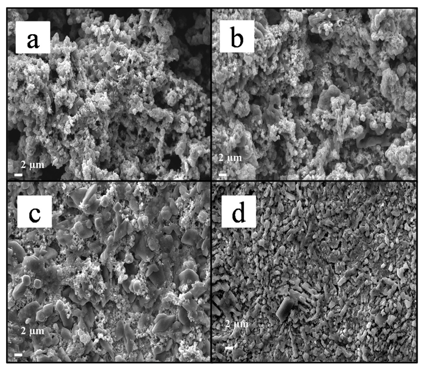
The morphology of the CZTS deposits formed at different pH after annealing is shown in Figs. 6 (a-d). It is clearly seen from Figs. 6 (a-d) that the samples deposited at pH 1.8 and 2 show dense deposits whereas the deposits formed at pH 2.5 and 2.8 are less dense. Figs. 7 (a-d) shows the deposits at higher magnification. It is seen from Figs. 7 (a-d) that the size and shape of the particles change with the electrolyte pH. The deposits formed at pH 1.8 and 2 shows the presence of more or less uniformly sized spherical or disc shaped particles. The deposits formed at pH 2.5 show the presence of less dense film consisting of larger sized particles. At pH 2.5, the size of the particles forming the deposit is predominantly non uniform and contains larger flaky particles. The change in the elemental composition of the deposits with pH is shown in Fig. 8. It is seen from Fig. 8 that the deposits formed at pH 2 and 2.5 are closer to the required stoichiometry. The deposits formed at pH 2.8 are copper rich. Increase in pH increases the copper composition whereas shows a continuous drop in tin composition. The atomic % of the elements along with the obtained stoichiometry is presented in Table 1. Figs. 9 a-d show the FEG-SEM cross sectional view of the deposits formed at different pH. It is seen from Figs. 9 a-d that the thickness of the deposits changes with pH. From the cross sectional images, thickness of the deposits formed at pH 1.8 and 2.5 are 19.8 ┬Ąm and 6.23 ┬Ąm respectively.
Fig.┬Ā6.
Lower magnification SEM images of the CZTS samples deposited from different pH electrolyte after annealing. a) 1.8 b) 2 c) 2.5 d) 2.8.
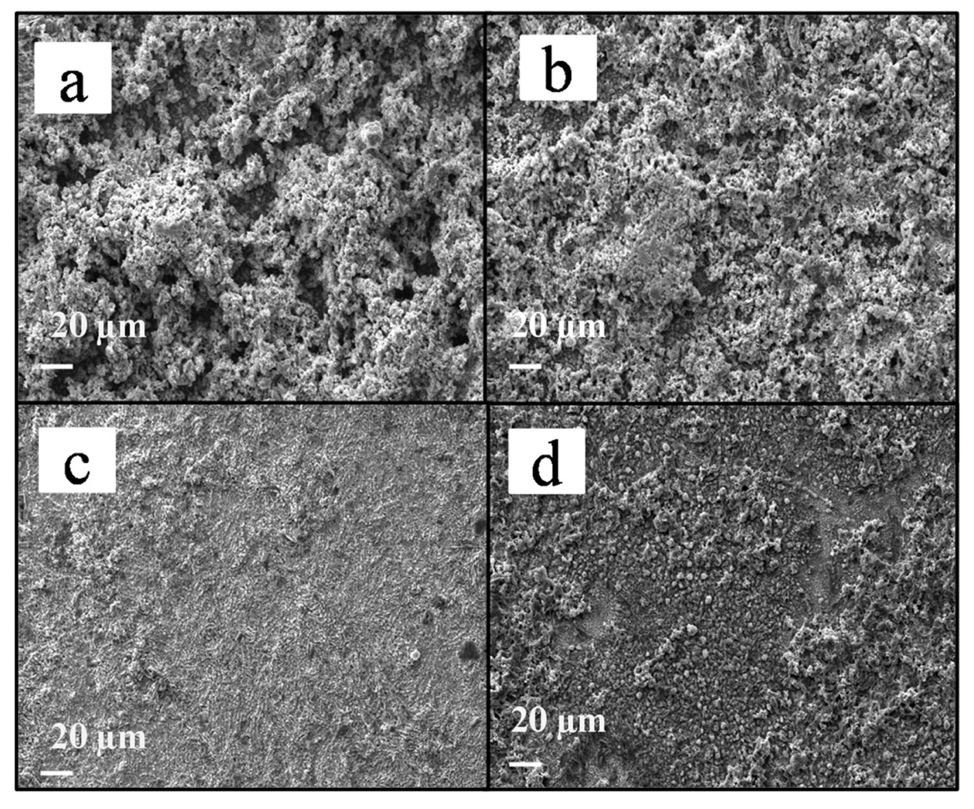
Fig.┬Ā7.
Higher magnification SEM images of the CZTS samples deposited from different pH electrolyte after annealing. a) 1.8 b) 2 c) 2.5 d) 2.8.


3.5 Transmission electron microscopy
Fig. 10a shows the TEM image of the CZTS deposits formed at pH 2 after annealing. It is seen from Fig. 10a, that the deposit consisted of particles of size less than 20 nm. It clearly shows the agglomeration of the particles which is also clear in the SEM images. Agglomeration of the particles is preferred in photovoltaic applications because aggregates are believed to reduce the recombination rate of photogenerated electrons [52]. The selected area electron diffraction (SAED) image for the same sample is shown in Fig. 10b. The image indicates a polycrystalline product as found in the XRD studies. The diffraction patterns correspond to the (101), (110), (112) and (202) planes of kesterite (JCPDS, Card no. 26-0575).

3.6 I-V characterization
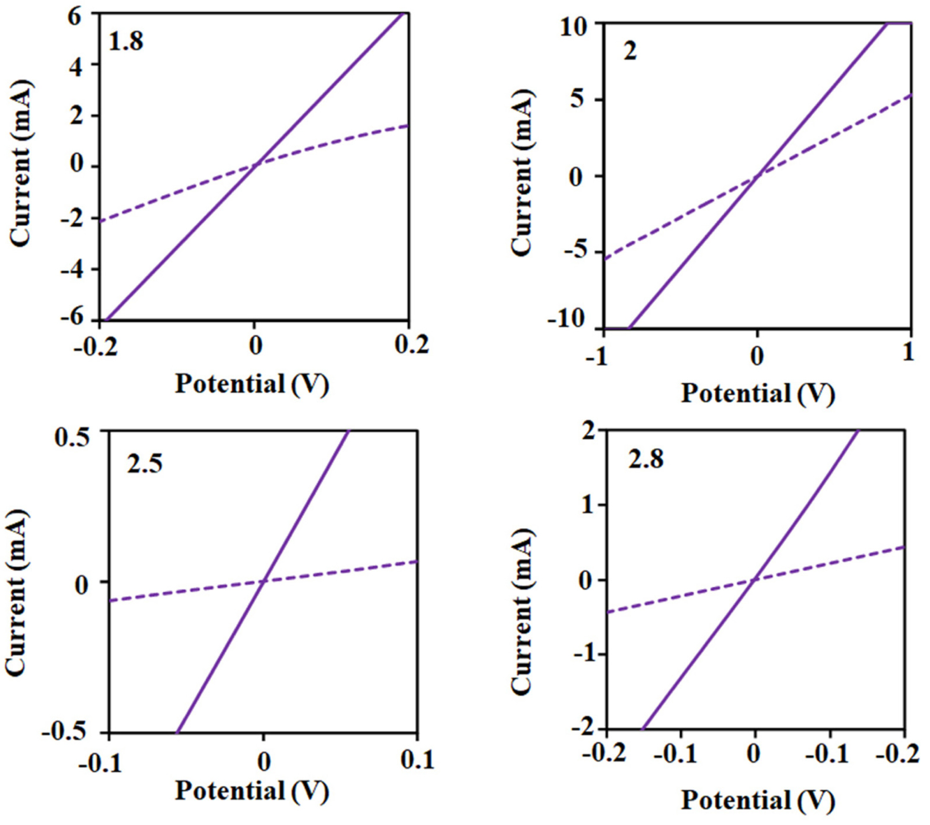
Fig. 11 shows the results of I-V characterization studies of ITO/CZTS/ITO system in the presence and absence of 200 W incandescent lamp. Annealed CZTS deposits were used in the studies. The I-V characterization studies give a straight line pattern in the potential range studied. Such a straight line feature indicates the Ohmic nature of the system [50]. The slope of the line decreases in the presence of light which shows that the deposit is suitable for solar cell applications [50]. The resistance values in the absence of light for the samples deposited at pH 2.5 and 2.8 are ten times higher than the resistance values in the presence of light source. The resistance values of the deposits in the presence and absence of light are shown in Table 2. The sample synthesized at pH 1.8 though deviates slightly from the stoichiometry, gives low resistance value when compared to other samples which could be due to the difference in the thickness of the deposits as observed from SEM images. The significant drop in the resistance values in the presence of light source clearly indicates the suitability of the synthesized deposits for solar cell absorber material. In a study on the electrodeposition of CZTS on FTO substrate using trisodium citrate as the complexing agent, deposits having electrical conductance of 52 ┬ĄS were synthesized [51]. The electrical conductance values of the CZTS deposits synthesized in this report are in the range of 9 mS to 33 mS in the presence of light. Thus, the deposits are suitable for solar cell applications.

3.7 Electrochemical impedance spectroscopy
Fig. 12 shows the Nyquist plots for the individual precursors with the complexing agent at pH 2.5. The Nyquist plot presents a depressed semicircle in the high frequency range which could be attributed to frequency dispersion due to surface inhomogeneity [53]. The low frequency end of the Nyquist plot for all the precursors presents a larger semicircle which is incomplete. The stability of the system was verified using KramerŌĆÖs Kronig Transformation (KKT). The KKT results for the experimental data are shown in Figs. 13 a and b which makes it clear that the system is stable, linear and causal. The Nyquist plots of all the precursors were modeled using the equivalent circuit shown in Fig. 14. Same equivalent circuit was used since the shape of the Nyquist plot is same for all the precursors. Since the Nyquist plot presents a depressed semicircle at high frequency end, a constant phase element (CPE) was chosen to model the system. The impedance of the CPE is given by Eq. 6. [54]

Fig.┬Ā12.
Nyquist plots for the individual precursors with 2 M sodium thiocyanate at pH 2.5.The potential used was ŌłÆ1 V. (Solid lines represent EEC fit).

Fig.┬Ā13.
Bode plots of the Kramers Kronig Transformation for the EIS data of the individual precursors with 2 M sodium thiocyanate at pH 2.5. (Solid lines represent KKT fit).

Fig.┬Ā14.
Electrical equivalent circuit employed to model the Nyquist plots obtained from the EIS runs of the individual precursors with 2 M sodium thiocyanate at pH 2.5.

In Eq. 6, the magnitude of CPE is represented by Qi with unit S sn; Žē is the angular frequency and j2 = ŌĆō1. The CPE exponent n, is the roughness parameter which takes values between 0 and 1 [54]. For an ideal capacitor, n = 1. The equivalent capacitance can be calculated from the elements of CPE using the Eq. 7.
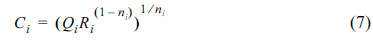
where Ri is the respective resistance. The equivalent circuit used to model the system consists of two CPE and three resistive elements. In the equivalent circuit, Rs represents the solution resistance, R1 and CPE1 corresponds to the charge transfer resistance for the M+ to M0, and double layer capacitance at the electrode-solution interface respectively, R2 is the charge transfer resistance for M2+ to M0 and CPE2 is the pseudo-capacitance due to deposited nuclei [51,53]. The values of the fit parameters are presented in Table 3. The rate controlling step for Zn, Sn and S is M+ to M which is indicated by higher values of R1 [55]. When compared to all the other elements, the charge transfer resistances related to sulfur are higher which shows that the cathodic process related to sulfur are the slowest [31]. The double layer capacitance represented by CPE1 does not change significantly for all the elements, whereas the CPE2 changes significantly with the highest value observed for zinc. This could be due to the rate of electrodeposition. The electrodeposition rate for zinc could be less since a higher value of capacitance will correspond to thinner deposit [54]. The relaxation time constant (Žä) also gives details on the electron lifetime which reveals information on the charge recombination rate and electron transfer rate which can be calculated from Eq. 8 [54,56]


4. Conclusions
Single step electrodeposition of CZTS for solar cell applications was studied. The qualities of the deposits synthesized at pH 2 were found to be good consisting of denser and thicker coating. The thickness of the deposits was found to decrease with the pH of the electrolyte. Compositional analysis by EDX revealed that nearly stoichiometric composition was obtained for the deposits synthesized at pH 2 and 2.5. The I-V characteristic studies showed that the films have good photo response with significant reduction in the resistance values in the presence of light. The EIS studies of the individual precursors at pH 2.5 indicate the presence of two time constants corresponding to multiple electron transfer steps with charge transfer resistance for sulfur being the highest when compared to other elements.


