


1. Introduction
The evolution of renewable energies over the last decade has surpassed all expectations. Among all renewable energy sources, solar energy is considered to be the most promising renewable energy sources for future energy needs due to its abundance and inexhaustibility. Solar cell is considered as a major candidate to get the sun’s energy, since it can directly convert sunlight to electricity [1,2].
Recently, use of photovoltaic solar cells leads to the research of new semiconducting thin films with acceptable efficiency. Metal chalcogenides are the most extensively studied ones such as tin sulfide [3-13]. This is one of the important IV-VI group semiconductors. In recent years, SnS films have attracted more considerable attention as low toxicity and costeffective materials [3-6]. SnS has been used in photovoltaic conversion, halographic recording media, photoconductors, near infrared detector and solar control device [7-10]. SnS films have large optical absorption coefficient (α >104 cm-1) which is higher than GaAs and CdTe films and a high photoelectric conversion efficiency can be up to 25% [3,11]. These phenomena show that SnS has a p-type conduction [5,8,12] and its electrical properties can be controlled by adding dopants, such as: Al, Ag, N, Sb and Cl [6,12]. Additionally, it shows a direct band gap of about 1.2-1.5 eV and an indirect band gap of about 1.0-1.1 eV to absorb the spectrum of solar radiation most efficiently in single junction solar cells [3,4,6,9,11].
SnS films have been deposited by various techniques such as atomic layer deposition [14], chemical bath deposition [15], hydrothermal method [16], mechanochemical route [17], silar method [18], spray pyrolysis [19], electron beam evaporation [20], sputtering [21], electrodeposition [1,12,22,23] and vacuum evaporation [4]. Among these techniques, electrodeposition is simple, inexpensive and convenient for large area deposition. It offers the possibility to control film thickness and morphology [22].
The use of additives in electroplating baths is very important. Many complexing agents have been investigated and sodium citrate is one of the most studied, especially in the electrodeposition of thin films such as ZnTe [24], ZnS [25], CuInSe2 [26,27], Cu(In,Ga)Se2 [28], Cu2ZnSnS4 [29], and SnTe [30]. Sodium citrate was added to the baths to reduce the cracks and improve the quality of the deposit [24]. Moreover, sodium citrate has proven to be a suitable, non toxic and cost effective compared to other additives [27, 28, 31]. However, to the best of our knowledge, there is no report in the literature about the electrodeposition of SnS films using sodium citrate as an additive.
Herein, the objective of this work is to elaborate SnS films by electrodeposition technique on Cu and ITO substrates using acidic solutions containing sodium citrate. The effects of sodium citrate on the electrochemical behavior of electrolyte bath containing tin chloride and sodium thiosulfate were investigated. Further, deposited films were characterized by X-ray diffraction (XRD), Fourier transform infrared spectroscopic (FTIR), scanning electron microscopy (SEM), optical, photoelectrochemical and electrical measurements.
2. Experimental
2.1 Reagents
All chemical reagents used in the present work were of analytical grade. Tin chloride dihydrate (SnCl2.2H2O, 98%), sodium thiosulfate pentahydrate (Na2S2O3.5H2O, 99.5%) and trisodium citrate dihydrate (Na3C6H5O7.2H2O, ≥ 99%) were obtained from Sigma Aldrich Pure Chemical Industries (Germany). The electrolytes were prepared with distilled water.
2.2 Electrochemical deposition of SnS thin films
Electrochemical experiments of SnS films were carried out using Princeton Applied Research model 273A Potentiostat-Galvanostat, connected to a conventional three-electrode glass cell consisting of ITO-coated glass (8-10 Ω/square, Sigma Aldrich) or Cu substrates as working electrodes; a platinum wire as a counter electrode and a saturated calomel electrode (SCE) was used as a reference electrode. All the potentials mentioned in this paper are expressed with respect to SCE. Prior to deposition, the substrates and the platinum wire were ultrasonically cleaned with HCl, acetone, and then rinsed with distilled water. The electrodeposition bath contained 20 mM SnCl2.2H2O, 100 mM Na2S2O3.5H2O and 20 mM Na3C6H5O7.2H2O. pH of solutions was adjusted to 1.0 ± 0.1 using 2 M HNO3. In addition, the deposition process was carried out at room temperature and prior to each experiment; the solutions were purged with purified nitrogen gas. Sodium citrate is used to stabilize Sn(II) ions in solution and avoid any precipitation [30-32]. SnH3L+ is the main Sn(II)-citrate complex at pH less than about 1.2. Where, L represents the tetravalent citrate ligand [30]. The concentrations of Sn(II) and sodium citrate were equal according to the following reaction (1):

The deposition potential for SnS films were determined from cyclic voltammetry data. Then, the films were electrodeposited at -1.25 V for 20 min and dried in air at 100°C.
2.3 Characterization techniques
Characterization of SnS films was carried out using different techniques. X-ray diffraction measurements were collected on a Bruker Discover D8 Diffractometer with a CuKα radiation (λ = 1.5406 Å). FTIR absorbance spectra were recorded on a Shimadzu FTIR-8000 series spectrophotometer in the wave-length range of 400-4000 cm-1. Scanning Electron Microscopy images was performed using a VEGA3, TESCAN. Optical transmittance of thin films was measured by a Perkin Elmer Lambda 950 UV-vis-NIR spectrometer in the wavelength range of 300-1500 nm. Photoelectrochemical measurements were carried out by cyclic voltammetry technique in a three electrode glass cell, using deposited SnS films as working electrodes, platinum wire as a counter electrode and a saturated calomel electrode as reference electrode in aqueous solution containing 100 mM Na2S2O3. A tungsten halogen lamp (100 W) was used as a light source. Electrical properties of SnS films were determined by a HMS 3000 Hall measurement system at room temperature. Silver paste was used at the corners of films to make four good contacts with probes. Thickness of the films was measured using Dektak stylus profilometer.
3. Results and Discussion
3.1 Electrochemical studies
3.1.1 Cyclic voltammetry
Fig. 1 shows the electrochemical behaviors of the Cu substrates in the solutions of sodium thiosulfate, tin chloride and their mixtures respectively. Fig. 1a shows the cyclic voltammetry of 0.1 M Na2S2O3 solution. Sodium thiosulfate is unstable in acidic media, which is reduced to colloidal sulfur according to the following reaction (2) [1,33,34]:
Fig. 1.
Cyclic voltammograms on Cu substrates in 0.1 M Na2S2O3 (a); 0.02 M SnCl2 (b) and 0.02 M SnCl2 + 0.1 M Na2S2O3 (c) at pH = 1 and scan rate 50 mV s-1.
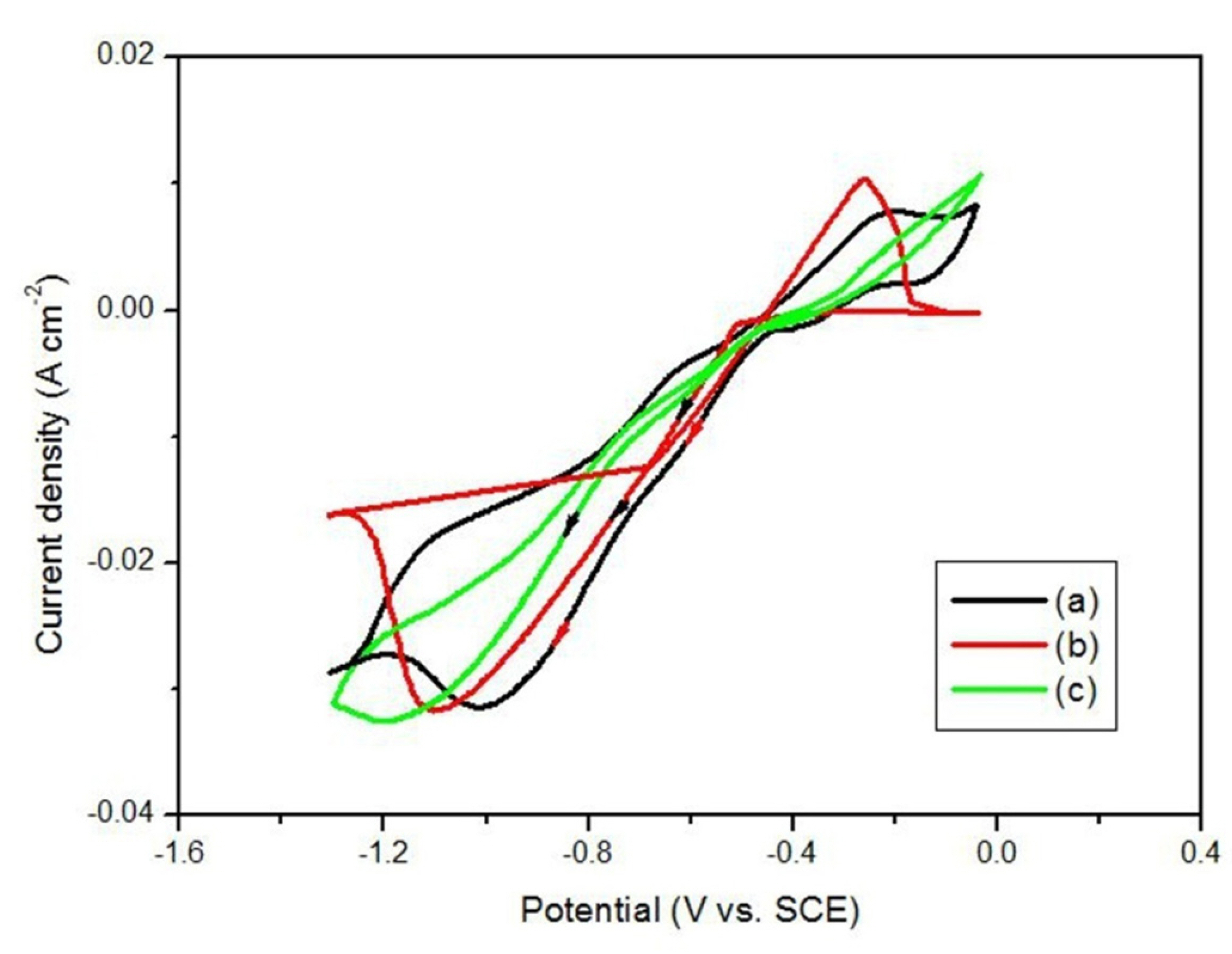

The sulfur adsorbed onto Cu substrate acts as an inhibitor of the hydrogen evolution. In the absence of Sn+2, the increase in current observed beyond a potential of ~ -0.5 V corresponds to the formation of dihydrogen sulfide. This corresponds to the following chemical reaction (3) proposed by Ghazali [1], Mathews [33] and Sharon [34]:
In the reverse scan, the anodic peak observed at about -0.21 V; could be attributed to the oxidation of S2O32- according to following reaction (4) [35]:
Fig. 1b represents the cyclic voltammetry of 0.02 M SnCl2 solution. In the forward scan, the cathodic current remains almost zero up to -0.5 V [36,37]. After which, a reduction wave can be observed at around -1.1 V, due to the reduction of tin ions to tin metal (reaction. 5).

The reverse scan crosses the forward scan at - 0.46 V, which characterized the nucleation and growth process [37]. The anodic peak is observed at about -0.26 V, this could be attributed to the dissolution of the deposited tin layer. The electrochemical behavior of tin in this work is similar to that reported by the previous authors [9,36-39].
Fig. 1c shows the cyclic voltammetry in the mixture of 0.02 M tin chloride and 0.1 M sodium thiosulfate solution. The cathodic peak observed at about - 1.2 V is due to the electroreduction of Na2S2O3 in the presence of Sn+2, which allows to the formation of SnS films on Cu substrate (reaction. 6). The electrochemical reaction of SnS formation of this work is similar to the mechanism of lead sulfide (PbS) reported by Mathews [33] and Sharon [34]:

During the reverse scan, the current oxidation could be attributed to the dissolution of SnS film.
Fig. 2 shows the comparaison of cyclic voltammograms in the mixture of 0.02 M tin chloride and 0.1 M sodium thiosulfate in solutions without (Fig. 2 (a, c)) and with 0.02 M sodium citrate (Fig. 2 (b, d)) on Cu and ITO substrates respectively. When, sodium citrate was added in solutions (Fig. 2 (b, d)), the current densities of cathodic peaks for the formation of SnS films increased comparatively with those without sodium citrate (Fig. 2 (a, c)). The ratio between cathodic peaks current densities with and without sodium citrate is about 1.4. These results indicate that sodium citrate does not block the active sites but activates the electrochemical reaction kinetics of SnS and acts as an accelerator for SnS deposition. This effect was also observed during the electrochemical preparation of SnS and nickel films in the presence of EDTA [1] and glycine [40] respectively.
Fig. 2.
Cyclic voltammograms of 0.02 M SnCl2 + 0.1 M Na2S2O3 (a, c) and 0.02 M SnCl2 + 0.1 M Na2S2O3 + 0.02 M Na3C6H5O7 (b, d) on Cu and ITO substrates at pH = 1 and scan rate 50 mV s-1.

A series of voltammograms of electrodeposited SnS films with sodium citrate on Cu and ITO substrates are shown in Fig. 3 (a, b) respectively at various scan rates. The difference between peaks potential and half peaks potential (ΔEp = Ep-Ep/2) varies with the scan rates from 0.298 to 0.553 V. According to Matsuda’s diagram [41], this significant difference indicates the irreversible kinetic reaction. The peak current densities of the cyclic voltammograms of SnS measured on Cu (Fig. 3a) are much higher than those on ITO (Fig. 3b), which implies that the reduction rate of SnS on ITO is slower than that on Cu substrate. Cathodic peaks current densities linearly increase with the increasing of scan rates (Insets of Fig. 3). This linearity of Jpc versus v1/2 plots suggests a diffusion controlled process for the electrochemical reaction of SnS deposited on both substrates.

3.1.2 Chronoamperometry
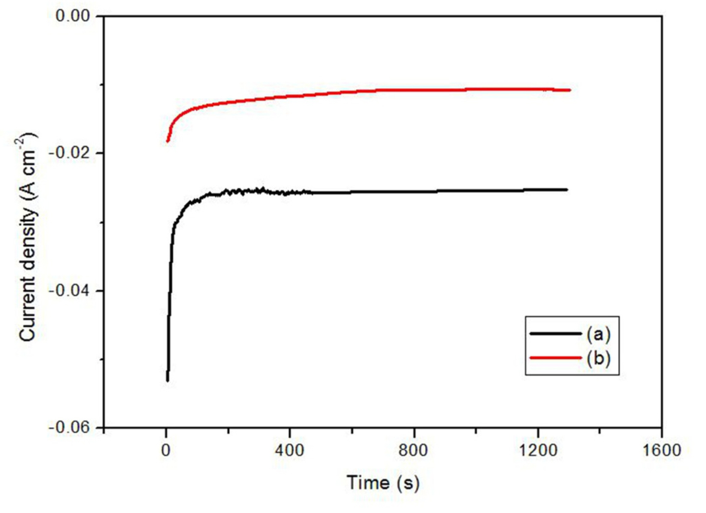
The chronoamperometric curves for the deposition of SnS films obtained at -1.25 V in the presence of sodium citrate on Cu and ITO substrates respectively are shown in Fig. 4 (a, b). The current densities measured by both substrates start with a high values which is assigned to a rapid nucleation and growth process. The current densities decrease as function of time due to a depletion of metal-ion concentrations close to the electrode surface and then stabilize with time corresponding to the diffusion limited current. The ratio between current densities measured on Cu and ITO substrates is about 3-fold which indicates that the reduction rate of SnS on Cu is faster than that on ITO substrates, as obtained from the results of cyclic voltammetry (CV).
3.2 Characterisation of SnS thin films
3.2.1 Structural analysis
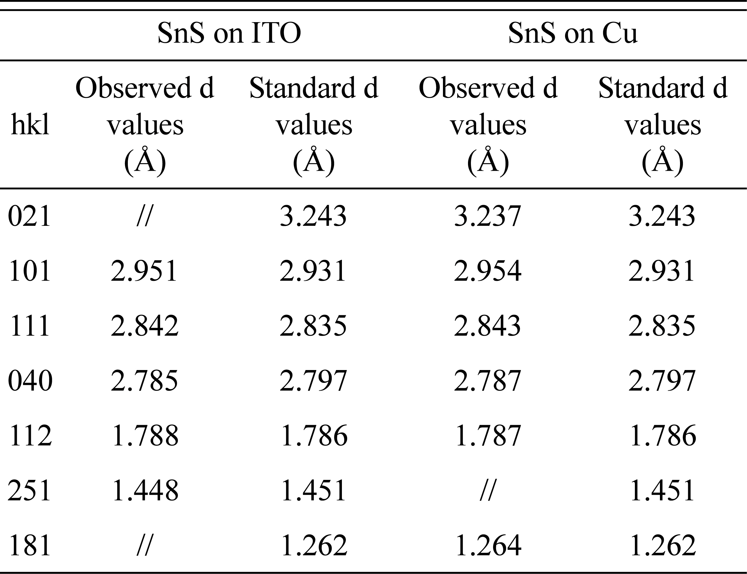
Thickness of SnS films was measured by Dektak stylus profilometer and was found to be 900 nm. Fig. 5 compares the XRD patterns of SnS films deposited without and with sodium citrate on ITO and Cu substrates. Fig. 5a shows the peaks at angular positions 2θ = 30.986° and 51.015°, corresponding to (111) and (112) diffractions of orthorhombic SnS phase. The observed peaks at 30.986° and 35.540° correspond to (222) and (400) planes of ITO substrate; the plane (222) of ITO is superimposed with (111) SnS plane. From Fig. 5b, the observed peaks of deposited SnS are related at 29.627°, 30.986°, 32.274°, 51.015° and 64.247°. These peaks are attributed to (101), (111), (040), (112) and (251) diffractions of orthorhombic SnS phase, respectively. The peaks observed in Fig. 5c at 2θ values of 27.531°, 29.631°, 30.987°, 32.276°, 51.013° and 75.230° respectively corresponding to (021), (101), (111), (040), (112) and (181) diffractions of orthorhombic structured SnS. The peak seen at 43.90° corresponds to (111) plane of Cu substrate. All peaks are in good agreement with JCPDS cards no 00-039-0354 and 00-014-620. The relative peak intensities of SnS (111), (040) and (112) planes on Cu substrate is more intense than those deposited on ITO substrates, which indicating that deposited films with sodium citrate on Cu substrate exhibited a higher degree of crystallinity.
Fig. 5.
XRD patterns of SnS films deposited without sodium citrate on ITO (a) substrate and with sodium citrate on ITO (b) and Cu (c) substrates.

From Fig. 5, the major peak (111) is the most dominant than other peaks and XRD analysis does not detect impurities such as SnO2 and SnS2. The average crystalline sizes (D) can be calculated by Scherrer’s formula (Eqn. 7), as follows [30]:

Where λ is the X-ray wavelength of CuKα radiation (1.5406 Å), θ is the Bragg’s angle (rad), and β is the experimental full-width half-maximum of the diffraction peak (rad). Estimated from the formula, the average grain size of deposited SnS without sodium citrate on ITO substrate was around 22.73 nm; but the average grain sizes of SnS with sodium citrate on Cu and ITO substrates were found to be 56.2 and 55.98 nm respectively. The XRD spectra (Fig. 5 (b, c)) correspond to the orthorhombic structure with average lattice parameters of a = 4.3399 Å, b = 11.1451 Å and c = 3.9895 Å, calculated from the least square fitting to the Bragg’s peaks. The crystal lattice parameters of SnS deposited on Cu as well on ITO match well with standard SnS (JCPDS card no. 00-039-354: its lattice constants a = 4.3291 Å, b = 11.1923 Å and c = 3.9838 Å) and there is a good agreement in the values of d interplanar spacing between observed and standard ASTM data (Table 1). These results indicated that deposited SnS with sodium citrate on Cu substrate exhibited a good crystalline structure if compared with that deposited on ITO substrate.
3.2.2 FTIR analysis
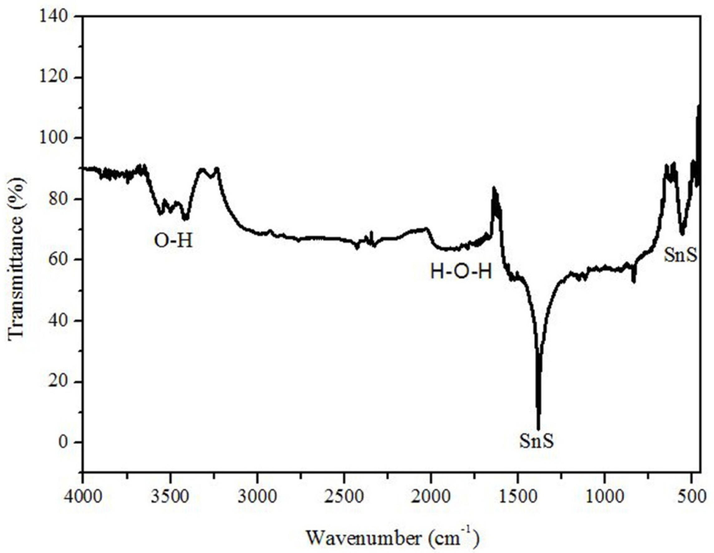
The FTIR spectrum of SnS films prepared with sodium citrate on Cu substrate between 400 and 4000 cm-1 is shown in Fig. 6. From this spectrum, it can be seen the appearance of bands at 560, 1384, 1659 and 3000-3650 cm-1. Strong and sharp peaks appear in the spectrum at 560 and 1384 cm-1 which are due to the characteristics of SnS. These bands are similar in positions, if compared with that obtained by Khel [42] and Henry [43]. The band at 1659 cm-1 is assigned to H-O-H bending of H2O molecules [44]. Broad band appeared in the range 3000-3650 cm-1 is assigned to stretching vibrations of O-H band from hydroxyl groups or absorbed water present on SnS surface [43]. Characteristic peaks of SnS in FTIR analysis are supported by XRD result (2θ = 30.986°), and they confirmed the presence of SnS films.
3.2.3 Morphological analysis
Fig. 7 (a-c) shows SEM micrographs of SnS films deposited without and with sodium citrate on Cu and ITO substrates. Micrograph 7a of SnS film deposited without sodium citrate on Cu substrate at -1.2 V revealed cracks and pinholes in the surface. Micrographs 7b and 7c show deposited SnS with sodium citrate at -1.25 V on Cu and ITO substrates respectively. Micrographs 7b are well covered with a smooth and uniform surface morphology consisting of spherical grain size. Micrograph 7c revealed non homogeneous surface with random oriented morphology. These results indicated that the addition of sodium citrate was improved the quality of deposited SnS on Cu than ITO substrates.

3.2.4 Optical properties
Optical properties of thin films are extremely important and band gap energy is one of the most extensively studied ones. Fig. 8 shows the plot of (αhν)2 versus photon energy (hν) of deposited SnS with sodium citrate. The linear nature of the graph indicates the existence of a direct transition. To estimate the optical band gap, the Tauc’s relation can be used [18] as follows (Eqn. 8):
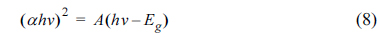
Where α is absorption coefficient, h is Planck’s constant (eV s), ν is photon energy (eV), A is a constant and Eg is the direct transition band gap. The absorption coefficient (α) was determined in the order of >104 cm-1. According to Tauc’s plot shown in Fig. 8, the optical band gap value was determined by extrapolating the linear portion of the plot with the energy axis ((αhν)2 = 0), where the intersection gives the value of Eg. Estimated direct band gap of SnS films is 1.3 eV, which is in good agreement with the values reported by [4,14]. This value makes it a suitable candidate as absorber film in solar cells applications.

3.2.5 Photoelectrochemical measurements
Fig. 9 shows the photoelectrochemical response of deposited SnS films on ITO substrates in dark (curve a) and under illumination (curve b). In dark, there is a negligible cathodic photocurrent. However, under illumination of the surface of deposited SnS, we observe an important cathodic photocurrent compared with that in the dark; suggests the existence of minority carriers (electrons), promotes the reduction of water producing H2 gas [45] at the semiconductor/electrolyte interface [1]. The cathodic photocurrent generation represents the typical behavior of p-type semiconductor conductivity with holes as the majority carriers [46,47]. SnS films deposited on ITO substrates showed the highest photoresponse compared to that obtained by Zainal [37] and Yongli [47].

3.2.6 Electrical properties
Electrical properties of SnS films with sodium citrate were examined by Hall Effect measurements at room temperature. SnS films showed a p-type electrical conductivity with carrier concentration of 2.6×1015 cm-3, mobility of 80 cm2V-1s-1 and a low electrical resistivity of 30 Ω cm. These values are in agreement with the data reported by Reddy [6] while their SnS films were prepared by spray pyrolysis technique.
4. Conclusions
In this paper, we report the electrodeposition of SnS thin films at -1.25 V for 20 min onto Cu and ITO substrates from a selected acidic solution containing 20 mM SnCl2, 100 mM Na2S2O3 and 20 mM sodium citrate. We found that the addition of sodium citrate has a strong effect on the electrochemical reaction kinetics and the quality of the deposited SnS films on Cu than ITO substrates. Thickness of deposited films was measured to be 900 nm. XRD data showed that SnS films on both substrates were polycrystalline, exhibiting orthorhombic structures and preferential orientations along (111) directions. However, SnS films with sodium citrate on Cu substrate exhibited a good crystalline structure if compared with that deposited on ITO substrates. FTIR results confirmed that the absorption peaks at 560 and 1384 cm-1 correspond to the characteristics of SnS films. SEM images revealed that SnS films on Cu substrate are well covered with a smooth and uniform surface morphology consisting of spherical grain size than deposited on ITO substrates. These films exhibited an optical band gap of 1.3 eV and had a high optical absorption coefficient (α > 104 cm-1) in visible-light region. p-type semiconductor conduction of SnS films was confirmed by photoelectrochemical and Hall Effect measurements. Electrical properties of SnS films showed a low electrical resistivity of 30 Ω cm, carrier concentration of 2.6×1015 cm-3 and mobility of 80 cm2 V-1s-1.
The obtained results are encouraging and showed that sodium citrate could be used as a suitable, non toxic and cost effective to prepare SnS films with good quality for hetero junction solar cells.


