


1. Introduction
Lead dioxide (PbO2) has been extensively investigated since its first use as a positive electrode in the lead-acid battery more than 150 years ago [1]. In addition to battery applications, it is broadly used as a metal oxide anode electrode due to its well-established advantages including a low cost compared to noble metals, easy to preparation, high electrical conductivity, good chemical stability in corrosive media, relatively large surface area and high over-potential for oxygen evolution reaction [2-4]. Currently, lead oxide is widely utilized in several electrochemical and industrial applications such as electro-catalyst (for example, for the formation of salicylic acid, 2-naphtol) [5,6], pH sensor [7], anodic material for ozone production [8-10], and oxidizing agent (for the oxidation of Cr3+ to Cr4+), and organic compounds in waste water treatments [11-13]. PbO2 has also been proposed as a component of dimensionally stable anode electrodes, in order to improve their electrocatalytic activity [14].
Traditionally lead oxide is prepared by pasted plate technology of which involves several consecutive and time-consuming processes. The alternative method involving electrodeposition of active materials directly onto the substrate offers several advantages over pasted plate technology; such as - it is faster method as lead ions can be directly oxidized to PbO2 [15], it can facilitate the use of light weight substrate as compared to lead alloy grid [16,17], and it is easy to control thickness and morphology of films [18]. Physicochemical behaviors as well as morphology of the electrochemically deposited PbO2 widely vary depending on the electrolyte used (conc. of Pb2+, pH, presence of anions and additives etc.), change of electrodeposition parameters (current density, temperature, and potential etc.), and substrate types (Pt, Au, Ti, Ni, graphite etc.) and their pretreatment conditions.
PbO2 is known to exist in two polymorphs: orthorhombic α-PbO2 generally deposits from basic and tetragonal β-PbO2 deposits from acidic solutions [19]. Lead dioxide electrodeposited on the reticulated vitreous carbon from acetate solution produced mainly α-PbO2 and that from nitrate solution produced β-PbO2 [20]. It has been reported [21] that electrochemical deposition of PbO2 on the Ni-substrate from electrolyte containing lead methanesulfonate and methanesulfonic acid produced compact β-phase only. The α-PbO2 having more compact structure possesses better contact between particles than that of β-PbO2; however, β-PbO2 possesses higher catalytic activity in dilute H2SO4 [22,23]. A report reveals that spontaneous surface modification occurred during cycling in acid media, and when a mixture of α- and β-PbO2 was cycled in H2SO4 the composition of the mixture changed with the decrease of α-PbO2 in the outer layer [24]. In another investigation, it has been reported that PbO2 deposited from nitrate solution had different phases of β-PbO2 depending on whether Au or Ti was used as substrate [25]. An investigation on electrodeposition of PbO2 on Pt, Au and Ti from solution containing Pb(NO3)2, HClO4, NaF, and methanol shows that low current density deposition produced uniform crystal grains with clear crystal edge, whereas higher current density produced deposition with rice-shape surface morphology [26].
Nickel is cheap, easily available, and has low density and sufficient strength together with good current collecting property due to high conductivity. On the other hand, Pb(NO3)2 is a cheap and easily available chemical with high aqueous solubility. Although some works have been conducted to electrodeposit PbO2 on Ni-substrate but the effect of different deposition conditions on the electrodeposition of PbO2 on nickel from acidic Pb(NO3)2 media is still unrevealed in extensive literature survey. In our work, we systematically investigated the effect of various deposition parameters such as Pb(NO3)2 concentration, anodic current density, and temperature on the surface morphology, crystal structure, and electrochemical behaviour of deposited PbO2 on the Ni-surface. The deposited PbO2 film has been characterised by deposition current efficiency and thickness measurements, and cyclic voltammetric experiments. Electrodeposition conditions greatly affect morphological and crystal structural states of the PbO2 deposit, and these in turn affect behaviour pattern of the deposit. Therefore, due emphasis has been given to investigate these two properties. Atomic Force Microscope (AFM) and Scanning Electron Microscope (SEM) have been used to investigate morphology, and X-ray Diffraction (XRD) study has been used to investigate crystal structural conditions.
2. Experimental
2.1. Material, chemicals, and their preparations
Commercially pure (purity 99.9%) 0.1 mm thick and 1 cm × 4 cm sized nickel coupons were used as substrate for PbO2 electrodeposition. Nickel coupons were polished with 1200 grit SiC paper, washed with liquid soap solution and immersed for 10 minutes in aqueous 1% NaOH solution. These were then cleaned in tap water, rinsed with distilled water, and finally dried in open air. The dry coupons were carefully covered with an insulating paint leaving 1 cm2 area exposed at one end for experiment. Small portions at both sides of the other end were also left exposed for electrical contact. These were further dried in an oven for 1 hour at 80°C. Weight of the dry coupons were accurately measured by an analytical balance, and preserved in a desiccator containing silica gel for subsequent experiment.
Lead nitrate (Qualikems, India), nitric acid (BDH, England), sodium hydroxide (E. Merck, India) and sulphuric acid (E. Merck, India) used in this work were analytical grade reagents. Aqueous 0.1 M, and 0.5 M Pb(NO3)2 solutions in 0.1 M HNO3 for electrodeposition, and 4.7 M H2SO4 solution for cyclic voltammetry were prepared by doubly distilled water.
2.2. PbO2 electrodeposition on Ni-substrate
Electrodeposition of PbO2 was carried out Galvanostatically using a precision controlled regulated DC Power Source (Model PS 303, Loadstar Electronics, Taiwan). The cell was a 100 mL Pyrex glass beaker containing 80 mL Pb(NO3)2 in HNO3 electrolyte placed on a thermostatically controlled hot plate having magnetic stirring facility (Model MS 300, Bante Instrument Ltd., China). The prepared Ni coupon connected to the positive terminal of the power source and another clean non-insulated coupon connected to the negative terminal were placed in parallel 2 cm apart in the cell solution in such a way so that the exposed surface was well immersed in the electrolyte, and the crocodile clips for electrical contact were well above the liquid level. A multimeter having zero resistance ammeter facility (Model 7045, Solartron Digital Multimeter, England) was connected in series for measuring current. After electrodeposition for the specified period (20 minutes) the anode was carefully washed in water and rinsed with distilled water. This was dried in open air and then in an oven for one hour at 80°C, and finally weighted accurately. The amount of PbO2 deposited was the difference of the weight of the coupon after and before electrodeposition. The deposition current efficiency and thickness were calculated using the following expressions.
where, n is no. of electron involved in the PbO2 deposition, W is deposition weight in g, F is Faraday constant (96478 coulombs), M is molecular weight of PbO2 in g, I is the current density in A cm-2 and t is time of deposition in second.
where, W is the weight of the deposited PbO2 in g, A is area of the plated surface in cm2 and D is density of PbO2 (9.38 g cm-3). The anode potential was measured by Saturated Ag|AgCl Reference Electrode (SSE) having Luggin capillary probe facility.
2.3. Cyclic voltammetric characterisation
Gill AC Impedance Analyser (ACM Instruments, England) was used for cyclic voltammetry. The experiment was conducted on a three-electrode glass beaker cell containing PbO2 deposited Ni as working electrode (WE), SSE with Luggin capillary probe as a reference electrode and Pt wire gauge as a counter electrode (CE). All voltammetric experiments were conducted in 4.7 M H2SO4 at 30°C temperature in static condition, and all potentials were reported against SSE. Experiments were conducted, and data collection and analyses were made with Gill AC software installed in a PC. Charge and discharge densities were calculated from the area under the peak or peak position divided by the scan rate following the procedure reported elsewhere [21]. The charge efficiency was obtained from the ratio of discharge density and charge density.
2.4. Morphology and crystal structure determinations
Model XEI-70 Park System Atomic Force Microscope (Suwon, Korea) and Model FEI Inspect S50 Scanning Electron Microscope (Oregon, USA) were used for the morphological and microstructural study. X-ray diffraction experiments were conducted with Model PW 3040 X’Pert PRO XRD System (Netherland) using Ni-filtered Cu-Kα radiation and “Cu-Tube” with maximum input voltage 60 KV and current 55 mA.
3. Results and Discussion
3.1. Current efficiency and thickness on deposition conditions
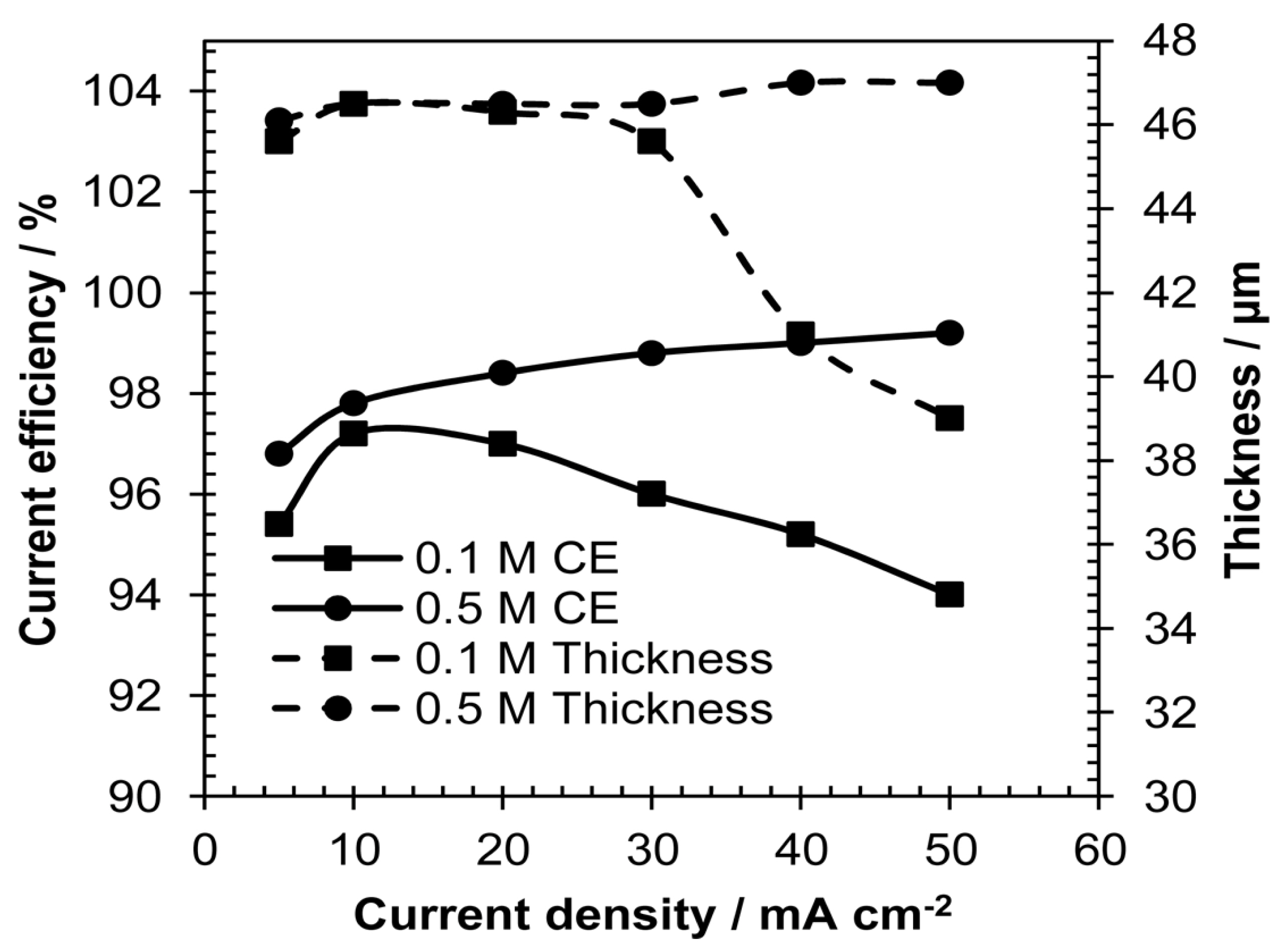
Lead dioxide (PbO2) was electrodeposited on the Ni-substrate from aqueous 0.1 M and 0.5 M Pb(NO3)2 solutions in 0.1 M HNO3. The effect of applied anodic current density and temperature on the current efficiency and film thickness were measured. Thickness measurements were carried out for constant 600 coulombs of applied charge density shown in Fig. 1. The current efficiency increased with increase of deposition current density for the deposition from 0.5 M Pb(NO3)2 solution, whereas it decreased for 0.1 M solution. The thickness remained almost unchanged (~46 μm) in the entire current density range for deposition from 0.5 M Pb(NO3)2 solution, whereas it decreased after 25 mA cm-2 current density for deposition from 0.1 M solution. Between two anodic reactions i.e., PbO2 film formation and oxygen evolution occur according to the following equations [27].
Fig. 1.
Effect of current density on current efficiency and thickness for PbO2 deposition on Ni from – (■) 0.1 M and (●) 0.5 M Pb(NO3)2 solutions in 0.1 M HNO3 at 30°C. Time and total charge density were 20 min. and 600 coulombs respectively.
And
Equation (4) is responsible for lowering of the current efficiency. The anode potential recorded with respect to SSE increased from initial 1.35 V to 2.2 V during electrodeposition from the low concentration Pb(NO3)2 solution at 50 mA cm-2 currentdensity due to concentration polarization effect. That big polarization was absent for the electrodeposition from 0.5 M Pb(NO3)2 solution. Oxygen evolution reaction starts at around 1.8 V which is more positive than the PbO2 formation potential [28]. Thus, low current efficiency for deposition from low concentration of Pb(NO3)2 at high current density is reasonable. The film thickness is not exactly proportional to the current density which reveals formation of more dense film of PbO2 from low Pb(NO3)2 solution.
The effect of temperature on current efficiency for deposition of PbO2 from 0.1 M Pb(NO3)2 solution at all three current densities i.e., 10 mA cm-2, 30 mA cm-2 and 50 mA cm-2 are shown in Fig. 2. The current efficiency rapidly decreased with the increase of temperature for deposition at 10 mA cm-2 current density; while the rate of decrease was very low at 50 mA cm-2 current density. This indicates that oxygen evolution was favored over PbO2 deposition at higher temperature when deposition was made at low current density. It has been reported [21,29-31] that for PbO2 deposition on Ni from 0.5 M Pb(CH3SO3)2 and 0.5 M CH3SO3H solution, low temperature favored deposition of α-PbO2, and high temperature favored deposition of β-PbO2. β-PbO2 has high conductivity due to high electron mobility, and high catalytic activity for oxygen evolution [32,33]. So, our results indicate that high temperature favored more β-PbO2 deposition, and low temperature favored more β-PbO2 deposition at low current density conditions. It is likely that more favorable oxygen evolution condition decreased current efficiency for PbO2 deposition with the increase of temperature.

3.2. Cyclic votammetric behaviors
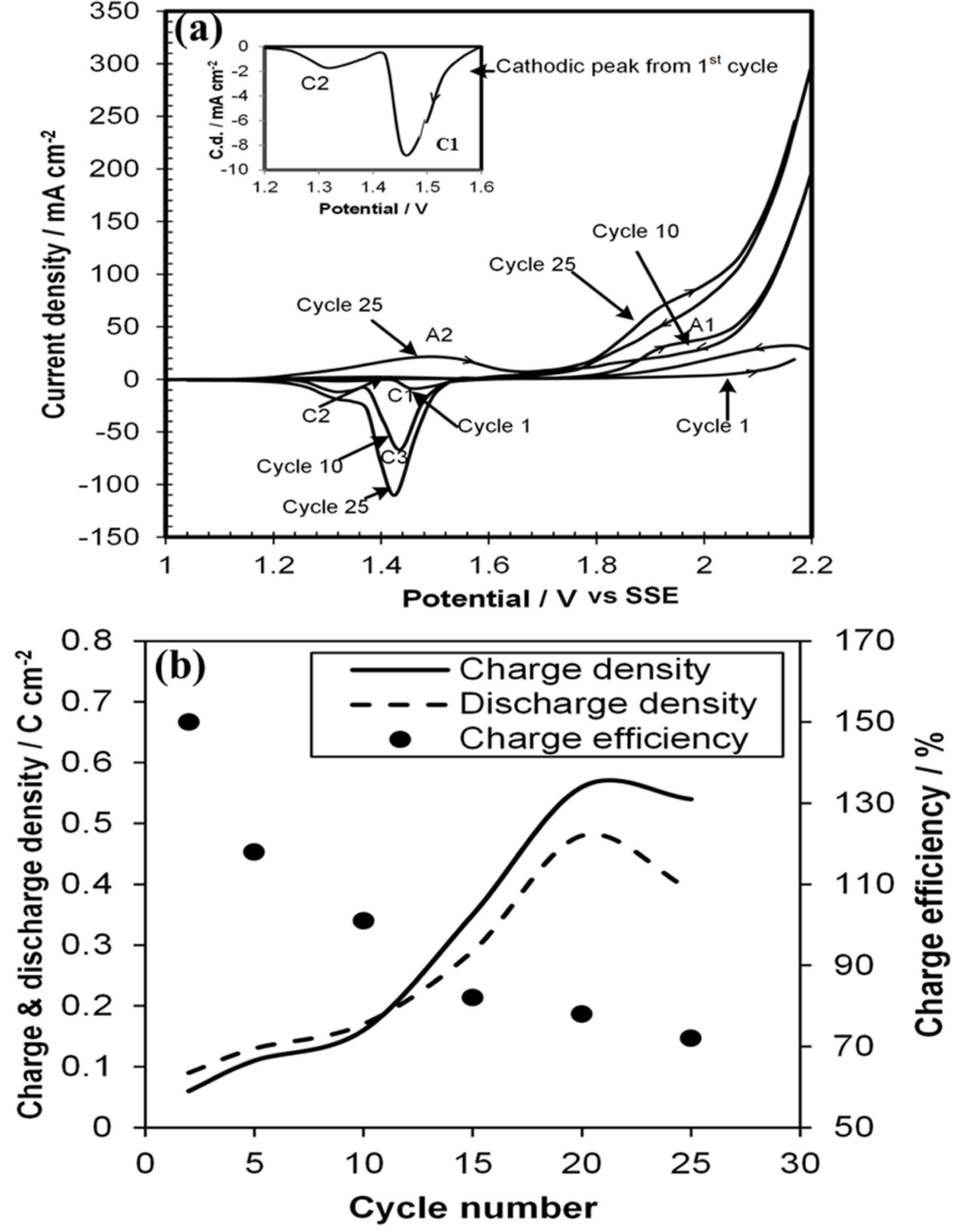
Cyclic voltammetric investigations were conducted on the deposited PbO2 in 4.7 M H2SO4 solution (lead-acid battery environment) between 1000 to 2200 mV at 30 mV S-1 scan rate. All potentials were measured with respect to SSE. For voltammograms shown in Fig. 3 deposition was made from 0.1 M Pb(NO3)2 solution for 20 minutes at 50 mA cm-2 current density. In Fig. 3a, the first cycle for the three voltammograms (1st, 10th and 25th cycles) started anodically at 1000 mV shows a small anodic current rise after approximately 1950 mV, and two cathodic peaks C1 and C2 (inset) at1460 mV and 1320 mV respectively. It is known [27] that between two polymorphic forms reduction of orthorhombic α-PbO2 to PbSO4 takes place at more positive potential than that for the reduction of tetragonal β-PbO2. So, peak C1 and C2 are due to reduction of α-PbO2 and β-PbO2 respectively. Normally α-PbO2 deposits from the basic solution and β-PbO2 deposits from the acidic solution as reported in the literature [19]. In fact, 0.1 M HNO3 is weak acidic solution. This may be reason for both α-PbO2 and β-PbO2 deposition in this acidic environment. The 10th cycle shows an anodic peak at around 1940 mV which merged with steep current rise after 2080 mV. It has been reported [28,34] that the oxidation of PbSO4 to PbO2 on Ni surface takes place at around 1800 mV, and oxygen evolution on PbO2 takes place at further positive potential. Thus, this peak was due to PbO2 formation and subsequent current rise was due to oxygen evolution. During cathodic scan a new big peak C3 (α+β-PbO2) appeared at more negative potential (1450 mV) than C1 with a shoulder of C2 peak. This peak was due to gradual shifting of C1 peak potential with the increase of cycle number i.e., α-PbO2 gradually converted to β-PbO2 which increases oxygen evolution properties from the start of 2nd cycle. All peak current densities and currents are several times bigger than that of the first cycle. The anodic scan of the 25th cycle shows a broad and shallow peak A2 at around 1450 mV for oxidation of substrate nickel to ultimate NiO(OH) formation as reported elsewhere [28,35,36]. The cathodic scan shows shifting of C3 peak potential to more negative value. All current rises are higher than those of 10th cycle. Increase of oxygen evolution current and other currents suggest formation of porous PbO2 due to repeated PbO2-PbSO4-PbO2 reactions. Noticeable nickel oxidation peak current indicates extension of pores up to Ni surface or falling apart part of PbO2 film from surface. The influence of cycle number on charge (PbSO4 → PbO2) and discharge (PbO2 → PbSO4) densities and charge efficiency are shown in Fig. 3b. The charge and discharge densities was obtained by calculating the area under the anodic and cathodic peaks in Fig. 3a divided by scan rate respectively. However, the charge efficiency was calculated from the ratio of discharge and charge current densities. This figure shows charge and discharge densities increased up to 20 cycles and then decreased. The decrease was due to parting away of PbO2 from the Ni surface. Initially, charge efficiency over was 140% which steadily decreased with the increase of cycle number. This indicates initially discharge density of PbO2 film was greater than charge density. This is similar result with literature [21] as they also obtained charge efficiency more than 100% for initial few cycles. This was due to increase of PbSO4 formation with cycle number, which was difficult for conversion to PbO2 due to non-conductivity. Densities of α-PbO2, β-PbO2 and PbSO4 are 9.87 g cm-3, 9.30 g cm-3 and 6.29 g cm-3 respectively [37]. Conversion of PbO2 to PbSO4 increased volume and produced internal stress for expansion. When PbSO4 was transformed to PbO2 volume contraction produced porosity resulting more surface area for charge-discharge as well as oxygen evolution reactions.
Fig. 3.
a. Cyclic voltammetry on PbO2 in 4.7 M H2SO4 at a scan rate of 30 mV s-1 and b. Effect of cycle number on charge discharge density & charge efficiency. Deposition was made on Ni from 0.1 M Pb(NO3)2 soln. in 0.1 M HNO3 at 50 mA cm-2 current density and 30°C temperature for 20 min.
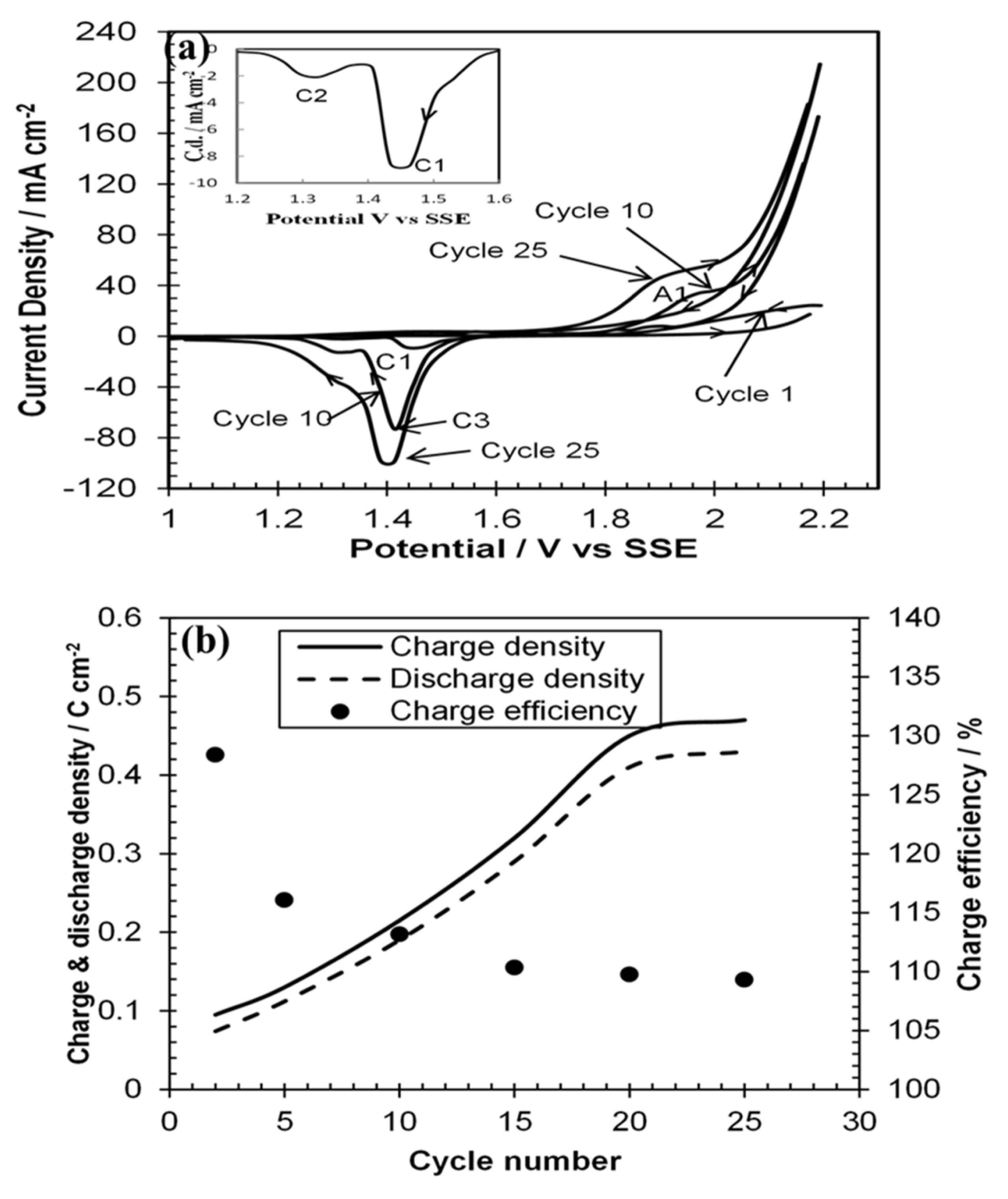
Cyclic voltammetric results for PbO2 electrodeposition from 0.5 M Pb(NO3)2 are shown in Fig. 4. The ratio of C1 and C2 height is 3.7 as obtained from Fig. 4a (inset of the 1st cycle) which is 5.9 for electrodeposition from 0.1 M Pb(NO3)2 solution. Which suggests that more α-PbO2 (approximately 85%) formed when deposition was made from 0.1 M Pb(NO3)2 solution compared to that (78%) for deposition from 0.5 M Pb(NO3)2 solution under identical deposition conditions. Density of α-PbO2 is higher than that of β-PbO2. This is one of the reasons for obtaining less thick deposit film from 0.1 M Pb(NO3)2 solution. However, all anodic and cathodic peak current heights are smaller in this case. Moreover, the 25th cycle does not show Ni oxidation currents, and the potential for C3 is more negative than that electrodeposition from electrolyte containing 0.1 M Pb(NO3)2. The charge efficiency attained a constant value (~112%) after 10th cycle in Fig. 4b. This revealed that electrodeposited of PbO2 from 0.5 M Pb(NO3)2 solution has better charge efficiency cycle number behavior. The oxygen evolution current density i.e., currents after 2000 mV (not shown) was always lower for deposition from 0.5 M Pb(NO3)2 solution. All of these suggest the presence of more β phase in the mixture of (α+β)-PbO2, and more compact PbO2 deposition from 0.5 M Pb(NO3)2 solution compared to that deposited from 0.1 M solution. Although β-PbO2 favors oxygen evolution reaction, nonetheless due to more compact film formation for deposition from 0.5 M Pb(NO3)2 solution less surface was exposed for oxygen evolution and charge-discharge reactions. This compact film was comparatively more adherent as evident from the absence of Ni oxidation peak.
3.3. AFM and SEM results
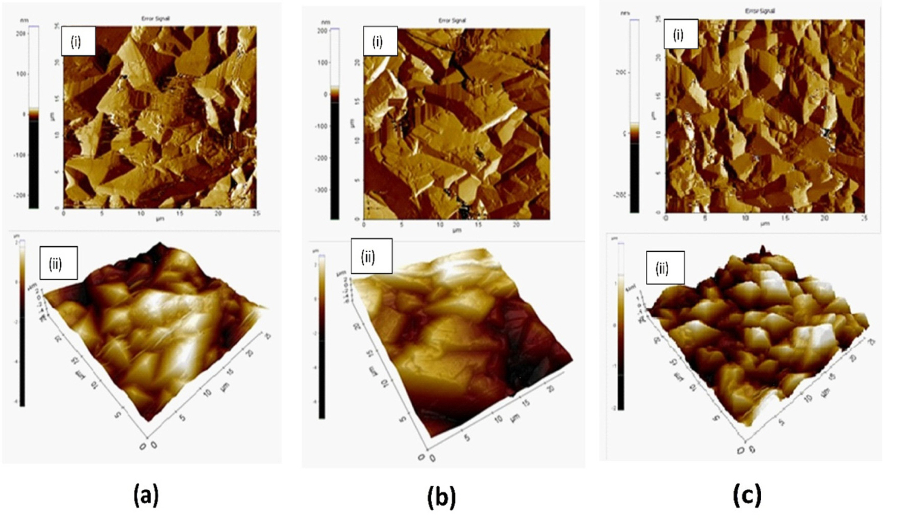
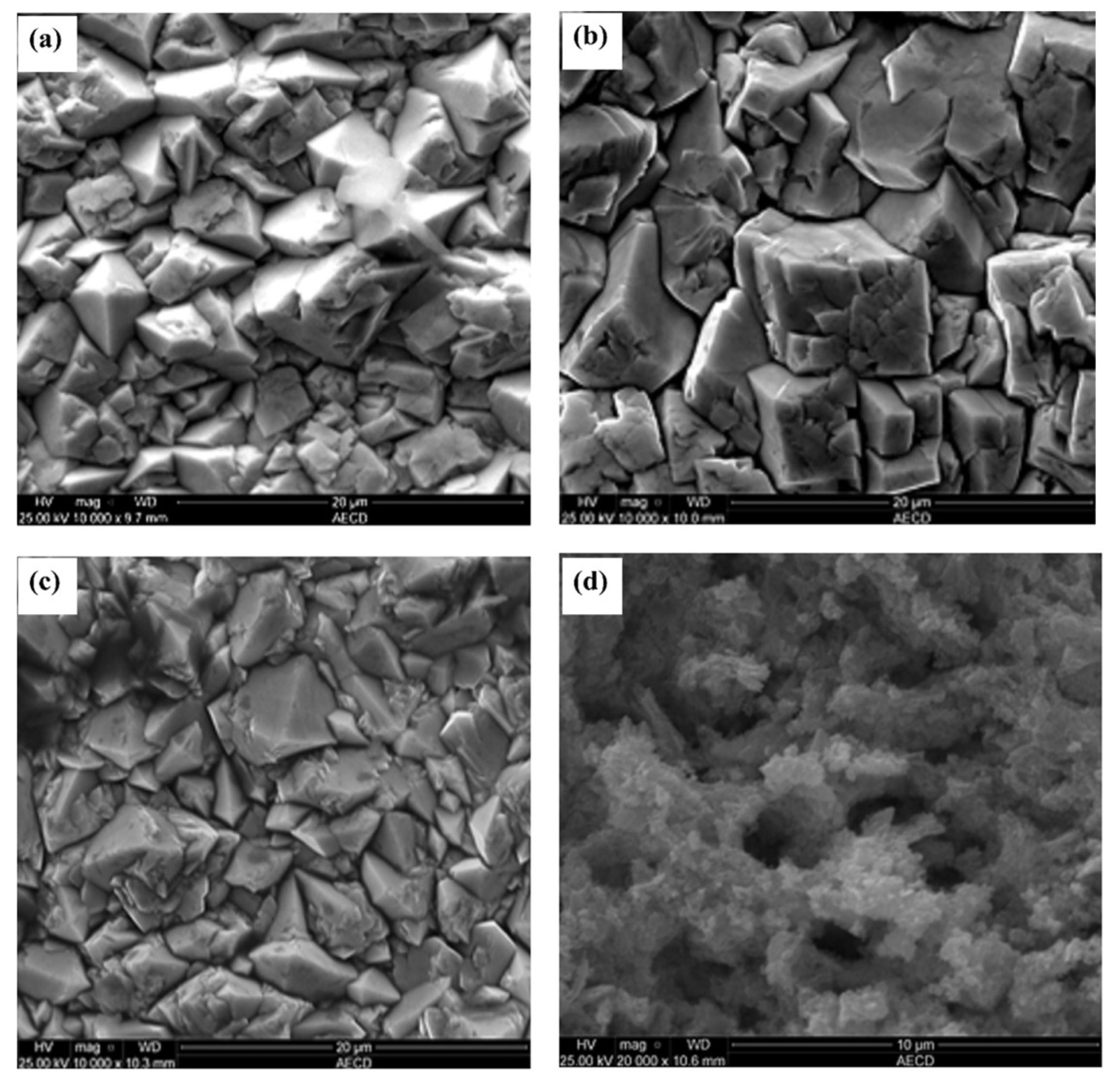
The AFM possesses higher resolution and is more versatile for depth profiling than SEM. AFM images of the PbO2 film deposited on Ni-surface from 0.1 M Pb(NO3)2 solution are shown in Fig. 5 –a, for 30°C and b, for 60°C electrodeposition, while Fig. 5-c, from 0.5 M Pb(NO3)2 solution at 30°C. In each case of Image (ii) is three-dimensional representation of the image (i). The grain size and surface roughness were slightly higher (8 μm and 1250 nm) for 60°C deposition than those for 30°C deposition (grain size 5 μm and roughness 902 nm). So, it could be argued that high current efficiency for 30°C and low current efficiency for 60°C electrodeposition conditions from 0.1 M Pb(NO3)2 are not related to the grain size and morphology of the deposited particles. However, for higher concentration deposition gave more smaller grain in size (avg. 4 μm) as well as lower roughness (620 nm) as compared to above two deposition conditions. Film thicknesses were approximately 79 μm and 74 μm for depositions from 0.5 M and 0.1 M Pb(NO3)2 solutions respectively. So, numbers of PbO2 layers were approximately 20 and 14 for deposition from these two solutions. This revealed that electrolytes i. e., H+ and HSO4¯ are less capable of penetrating into the film deposited from 0.5 M Pb(NO3)2 solution during PbSO4-PbO2-PbSO4 conversion process in cyclic voltammetry as we observed earlier in cyclic voltammetry experiment. Fig. 6-a and -b were SEM images of the PbO2 deposited from 0.1 M Pb(NO3)2 solution at 30°C and 60°C respectively, while 6-c and -d were PbO2 deposited from 0.5 M Pb(NO3)2 solution before and after cyclic voltammetry. The grain produced were bigger in size for higher temperature condition although both were deposited from same 0.1 M Pb(NO3)2 solution. While Relatively irregular pyramid-shape, broken in nature (like broken pebbles) with sharp-edges grain were produced from 0.5 M Pb(NO3)2 solution as shown in Fig. 6-c. The results from SEM are in well agreement with AFM study. SEM image (Fig. 6d) after 25 cycles of cyclic voltammetry shows that regularshape grains broke completely with the formation of small, irregular shape loosely adhered flappy deposits with many big and deep holes.
3.4. XRD on PbO2 deposits
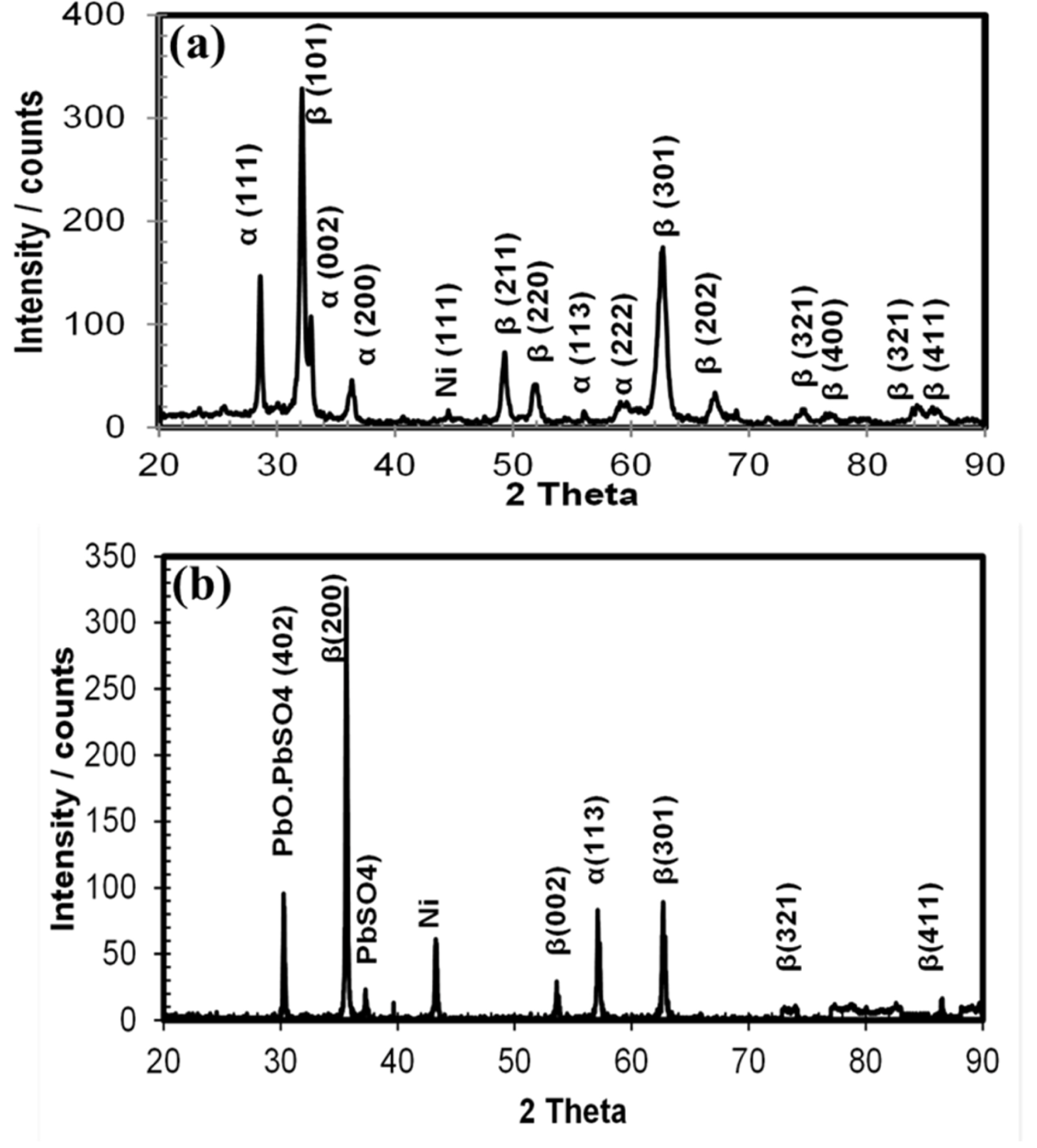
X-ray diffractograms of the PbO2 deposited on Ni-surface from electrolytes containing 0.1 M Pb(NO3)2 in 0.1 M HNO3 are shown in Fig. 7 for - a, 10 mA cm-2 current density and 30°C; b(i), 50 mA cm-2 current density and 30°C, and b(ii) 50 mA cm-2 current density and 60°C electrodepositions. For ‘a’ two intense main peaks at 28.5° and 32.8° are from (111) and (002) planes of α-PbO2, for ‘b(i)’ four intense peaks at 28.5°, 32.07°, 52.3° and 62.6° are from α(111), β(101), β(220) and β(301) planes, and for b(ii) the two most intense peaks at 59.8° and 62.6° are from α(222) and β(301) planes respectively. Relatively β-PbO2 peak height increased when current density was increased to 50 mA cm-2, and temperature was raised from 30°C to 60°C. These indicate that high current density and high temperature favored deposition β-PbO2. Fig. 8 shows diffractograms of PbO2 deposited from 0.5 M Pb(NO3)2 solution at 30°C – a, before and b, after 25 cycles of voltammetry as mentioned in Fig. 4. The β(101) peak at 32.07° in ‘a’ is the largest one. Even the 2nd largest broad β(301) peak is bigger than the biggest α(111) peak. These are clear indication that high concentration of Pb(NO3)2 at 30°C favored deposition of more β-PbO2. In ‘b’ the most intense peak is from β(200) plane at 36° and the 2nd biggest peak is for PbO.PbSO4 at 30°. Peaks for α-PbO2 are significantly smaller like the case before cyclic voltammetry. Ni (111) peak at 44.5° is much bigger than any case. This indicates exposure of Ni surface after cyclic voltammmetry.
Fig. 7.
X-ray diffractograms of PbO2 deposited for 20 min on Ni from 0.1 M Pb(NO3)2 solution in 0.1 M HNO3 at current densities and temperatures – a, 10 mA cm-2 and 30°C; b(i), 50 mA cm-2 and 30°C, and b(ii) 50 mA cm-2 and 60°C.
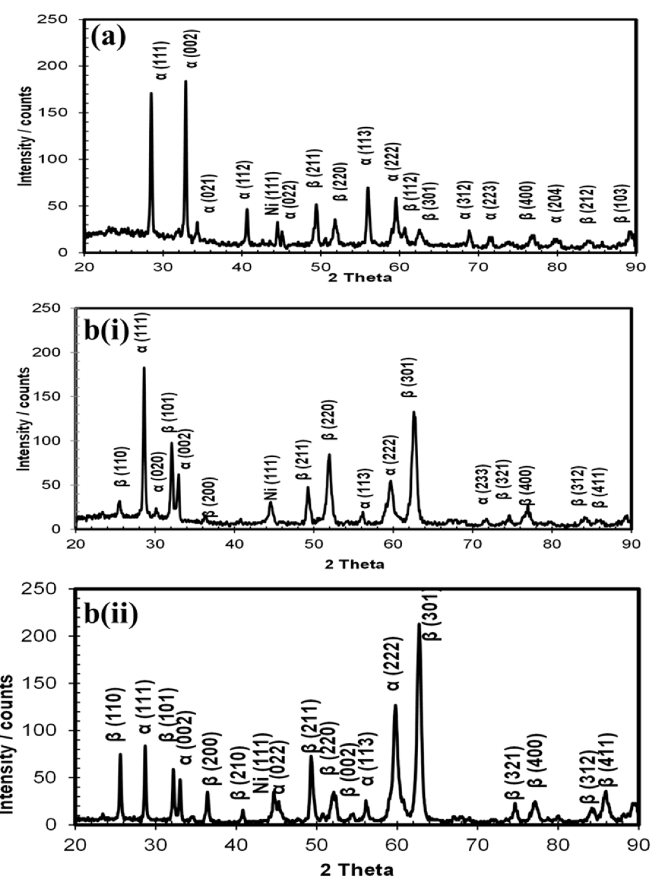
Fig. 8.
X-ray diffractograms of PbO2 deposited on Ni for 20 min from 0.5 M Pb(NO3)2 solution in 0.1 M HNO3 at 50 mA cm-2 current density & 30°C temperature – (a) before and (b) after 25th cycles as in Fig. 4.
4. Conclusions
Both α- and β-PbO2 films were electrodeposited on nickel surface from acidic solution of Pb(NO3)2. However, high Pb(NO3)2 concentration, high current density and high temperature resulted increase of β-PbO2 content in the deposit. Deposition from lower concentration of lead nitrate at higher current density produced mostly porous α-PbO2 due to innumerous amount of oxygen evolution. Higher temperature and lower lead nitrate solution condition produced larger grain than from deposition at lower temperature and higher solution concentration. More amount of β-PbO2 in the deposit gives lower charge discharge current densi ty due to their high adherence properties. Both types of PbO2 were converted into flappy deposit arising some pores during cycling. PbO2 deposited on nickel surface from the Pb(NO3)2 solution in 0.1 M HNO3 in the present experimental conditions could not significantly improve charge-discharge cycles in the lead-acid battery environment.


